SLLSET1B January 2016 – February 2017 SN75LVPE802
PRODUCTION DATA.
- 1 Features
- 2 Applications
- 3 Description
- 4 Revision History
- 5 Description (continued)
- 6 Pin Configuration and Functions
- 7 Specifications
- 8 Detailed Description
- 9 Application and Implementation
- 10Power Supply Recommendations
- 11Layout
- 12Device and Documentation Support
- 13Mechanical, Packaging, and Orderable Information
Package Options
Refer to the PDF data sheet for device specific package drawings
Mechanical Data (Package|Pins)
- RTJ|20
Thermal pad, mechanical data (Package|Pins)
- RTJ|20
Orderable Information
9 Application and Implementation
NOTE
Information in the following applications sections is not part of the TI component specification, and TI does not warrant its accuracy or completeness. TI’s customers are responsible for determining suitability of components for their purposes. Customers should validate and test their design implementation to confirm system functionality.
9.1 Application Information
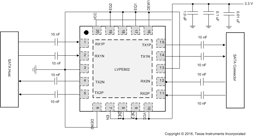
The SN75LVPE802 can be used for SATA applications as well as SATA Express applications. The device supports SATA Gen1, Gen2, and Gen3 applications with data rates from 1.5 to 6 Gbps. The built-in equalization circuits provide up to 13 dB of equalization at 3 GHz. This equalization can support SATA GEN2 (3 Gbps) applications over up to 50 inches of FR-4 material. The same 13 dB equalizer is suited to SATA Gen3 (6 Gbps) applications up to 40 inches of FR4.
In addition to SATA applications, the SN75LVPE802 can support SATA Express applications. SATA Express provides a standardized interface to support both SATA (Gen1, Gen2, and Gen3) and PCI Express (PCIe 1, 2 and 3).
All applications of the SN75LVPE802 share some common applications issues. For example, power supply filtering, board layout, and equalization performance with varying interconnect losses. Other applications issues are specific, such as implementing receiver detection for SATA Express applications. The Typical Application examples demonstrate common implementations of the SN75LVPE802 supporting SATA, as well as SATA Express applications.
9.2 Typical SATA Application
This typical application describes how to configure the EQ, DE, and DEW configuration pins of the SN75LVPE802 device based on board trace length between the SATA Host and the SN75LVPE802 and the SN75LVPE802 and SATA Device. Actual configuration settings may differ due to additional factors such as board layout, trace widths, and connectors used in the signal path.

9.2.1 Design Requirements
Typically, system trace length from the SATA host to the SN75LVPE802 device and trace length from the SN75LVPE802 device to a SATA device differ and require different equalization and de-emphasis settings for the host side and device side.
For example:
- A system with a 6-inch trace from the SN75LVPE802 device to a SATA host may set EQ1 (Rx1±) to 7 dB, and DE2 (Tx2±) to –2 dB and DEW2 (Tx2±) to long pulse duration.
- The same system with a 1-inch trace from the SN75LVPE802 device to a SATA HDD may set EQ2 (Rx2±) to 0 dB, and DE1 (Tx1±) to 0 dB and DEW1 (Tx1±) to short pulse duration.
Refer to Application Curves for recommended EQ, DE and DEW settings based on trace length. It is highly recommended to add both pullup- and pulldown-resistor options in the layout to fine-tune the settings if needed. Input Signal Characteristics:
- Data Rate: 6 Gbps
- Pattern: PRBS7
- No pre-emphasis
- Signal amplitude: 500 mVpp
- 18-inch SMA cable from test equipment to input and output trace
 Figure 26. Measurement Set-up
9.2.2 Detailed Design Procedure
9.2.2.1 Equalization Configuration
Each differential input of the SN75LVPE802 device has programmable equalization in the front stage. The equalization setting is shown in Table 1. The input equalizer is designed to recover a signal even when no eye is present at the receiver and effectively supports FR4 trace input from 3 inches to greater than 24 inches at SATA 6 Gbps speed.
9.2.3 De-emphasis Configuration
The SN75LVPE802 device provides the de-emphasis settings shown in Table 1 and Table 2. TX and Rx EQ and DE Pulse-Duration Settings. De-emphasis is controlled independently for each channel and is set by the DE1, DE2, DEW1 and DEW2 pins of the SN75LVPE802 device.
9.2.4 Application Curves
Typical application curves correspond to SATA application at 6 Gbps.
9.2.4.1 SN75LVPE802 Equalization Settings for Various Input Trace Length
.gif)
| Input Trace Length = 6 in. | ||
| EQ1, EQ2 Setting = 0 (7 dB) |
.gif)
| Input Trace Length = 12 in. | ||
| EQ1, EQ2 Setting = 0 (7 dB) |
.gif)
| Input Trace Length = 24 in. | ||
| EQ1, EQ2 Setting = 0 (7 dB) |
.gif)
| Input Trace Length = 3 in. | ||
| EQ1, EQ2 Setting = NC (0 dB) |
.gif)
| Input Trace Length = 6 in. | ||
| EQ1, EQ2 Setting = 0 (7 dB) |
.gif)
| Input Trace Length = 12 in. | ||
| EQ1, EQ2 Setting = 0 (7 dB) |
.gif)
| Input Trace Length = 24 in. | ||
| EQ1, EQ2 Setting = 0 (7 dB) |
.gif)
| Input Trace Length = 36 in. | ||
| EQ1, EQ2 Setting = 1 (14 dB) |
9.2.4.2 SN75LVCP802 De-emphasis Settings For various Output Trace Lengths
.gif)
| Output Trace Length = 0 in. | DE, DE2 Setting = 0 (0 dB) |
| DEW1, DEW2 Setting = 0 (Short pulse duration) | |
.gif)
| Output Trace Length = 6 in. | DE, DE2 Setting = 1 (-2 dB) |
| DEW1, DEW2 Setting = 1 (Long pulse duration) | |
.gif)
| Output Trace Length = 12 in. | DE, DE2 Setting = NC (-4 dB) | |||
| DEW1, DEW2 Setting = 1 (Long pulse duration) | ||||
9.3 SATA Express Applications
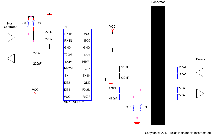
 Figure 44. SATAe Reference Schematic
9.3.1 Detailed Design Procedure
Figure 44 is a reference schematic of a SATAe implementation using the SN75LVPE802. With a SATAe design, both SATA and PCI Express must be supported. SATAe supports both cabled and direct connections. Using a cabled application as an example, the SATAe power connector includes an Interface Detect (IFDet, power connector pin P4) signal that indicates whether a SATA client or a PCIe client is connected.
When the SATAe host determines that a PCIe client is connected, the SATAe host performs receiver detection. Receiver detection determines the presence of a client by detecting the load impedance. The transmitter performs a common mode voltage shift, and measures the rate at which the voltage at the transmitter output changes. The rate of change indicates if a client is present (fast charging when a low impedance load is present, or slow charging when the load is open or high impedance). With the implementation in Figure 44, 330-Ω pulldowns have been inserted between the host and the SN75LVPE802. The pulldown resistors indicate to the host that a client is present. While an actual client would be expected to have an active load of 50 Ω single ended, the 330 Ω is chosen here to meet two requirements. The 330 Ω is low enough to force the SATAe host to decide that a receiver is present, while also high enough to only marginally affect the load when the SN75LVPE802 is active, and presenting a 50-Ω load. With the 50 Ω and 330 Ω are both present, the parallel combination of 43 Ω is satisfactory for most applications.
Assuming that the SATAe host has detected (via IFDet) that a SATA client is present, the SATAe host communicates with the client via the SN75LVPE802. The SATA standard does not have a receiver detection mode as is present in PCIe. A SATA host does use OOB signaling to communicate identification information. The SN75LVPE802 incorporates an OOB detector in order to support OOB signaling through the device. The OOB detector drives a squelch circuit on the SN75LVPE802 output transmitter. (See OOB/Squelch for more details on the OOB/Squelch circuitry.)
Returning to Figure 44, there is a 200-nF AC coupling capacitors on the device or client side of the interface. These capacitors allow interfacing to both SATA and PCIe clients. In the case of a PCIe client, the 200 nF is within the acceptable range for all PCIe devices. When a SATA client is present, the 200 nF capacitor has little effect on the overall link, as it appears in series with the 12-nF (max) AC coupling capacitor incorporated into the SATA client. The 200 nF in series with the 12 nF presents an effective capacitance of 11.3 nF, as expected less than the 12-nF maximum permitted.
9.3.2 PCIe Applications
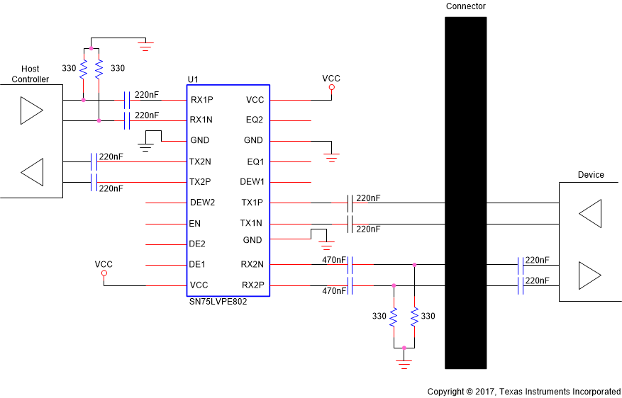
PCIe-only applications are implemented in a manner very similar to SATA Express applications as covered in Detailed Design Procedure. Looking at Figure 45 and comparing it to the SATA Express application in Figure 8 20 SATAe Reference Schematic, a single change is noted. For PCIe applications the 220 nF AC-coupling capacitors on the Host-to-Device link are relocated from the Device side of the connector to the Host side. No other changes are required.
 Figure 45. SN75LVPE802 PCIe Reference Schematic
.gif)
.gif)
.gif)
.gif)
.gif)