SLLSET1B January 2016 – February 2017 SN75LVPE802
PRODUCTION DATA.
- 1 Features
- 2 Applications
- 3 Description
- 4 Revision History
- 5 Description (continued)
- 6 Pin Configuration and Functions
- 7 Specifications
- 8 Detailed Description
- 9 Application and Implementation
- 10Power Supply Recommendations
- 11Layout
- 12Device and Documentation Support
- 13Mechanical, Packaging, and Orderable Information
Package Options
Refer to the PDF data sheet for device specific package drawings
Mechanical Data (Package|Pins)
- RTJ|20
Thermal pad, mechanical data (Package|Pins)
- RTJ|20
Orderable Information
8 Detailed Description
8.1 Overview
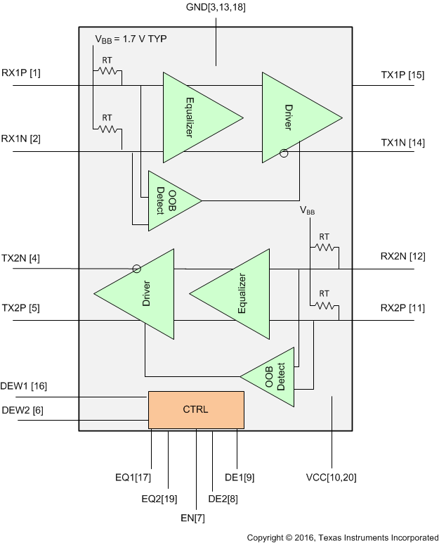
The SN75LVPE802 is a dual channel equalizer and redriver. The device operates over a wide range of signaling rates, supporting operation from DC to 8 Gbps. The wide operating range supports SATA Gen 1, 2, 3 (1.5 Gbps, 3.0 Gbps, and 6.0 Gbps respectively) as well as PCI Express 1.0, 2.0, 3.0 (2.5 Gbps, 5.0 Gbps, and 8.0 Gbps). The device also supports SATA Express (SATA 3.2) which is a form factor specification that allows for SATA and PCI Express signaling over a single connector.
8.2 Functional Block Diagram

8.3 Feature Description
8.3.1 SATA Express
SATA Express (sometimes SATAe) is an electro-mechanical standard that supports both SATA and PCI Express storage devices. SATAe is standardized in the SATA 3.2 standard. The standard is concerned with providing a smooth transition from SATA to PCIe storage devices. The standard provides for standardized cables and connectors, and muxes the PCIe and SATA lanes at the host side so that either SATA compliant or PCIe compliant devices may operate with a host.
SATAe provides support for SATA1, SATA2 and SATA3 devices (operating from 1.5 Gbps to 6.0 Gbps), as well as PCIe1, PCIe2 and PCIe3 devices (operating from 2.5 Gbps to 8.0 Gbps).
The SN75LVPE802 provides for equalization and re-drive of a single channel input signal complying with any of the SATA or PCIe standards available with SATAe.
The SATAe standard provides for a mechanism for a host to recognize and detect whether a SATA or PCIe device is plugged into the host. See the Typical SATA Application section for the details of the SATA Express Interface Detect operation.
8.3.2 Receiver Termination
The receiver has integrated terminations to an internal bias voltage. The receiver differential input impedance is nominally 100 Ω, with a ±15% variation.
8.3.3 Receiver Internal Bias
The SN75LVPE802 receiver is internally biased to 1.7 V, providing support for AC coupled inputs.
8.3.4 Input Equalization
The SN75LVPE802 incorporates programmable equalization. The EQ input controls the level of equalization that is used to open the eye of the received input signal. If the EQ input is left open, or pulled LO, 6 dB (at 3 GHz) of equalization is applied. When the EQ input is HIGH, the equalization is set to 13 dB (again at 3 GHz). Table 1 shows the equalization values discussed.
Table 1. EQ and DE Settings
| EQ1 OR EQ2 | CH1 OR CH2 EQUALIZATION dB (at 6 Gbps) |
CH1 OR CH2 EQUALIZATION dB (at 8 Gbps) |
DE1 OR DE2 | CH1 OR CH2 DE-EMPHASIS dB (at 6 Gbps) |
|---|---|---|---|---|
| NC (default) | 0 | 0 | NC (default) | -4 |
| 0 | 6 | 7 | 0 | 0 |
| 1 | 13 | 15 | 1 | -2 |
8.3.5 OOB/Squelch
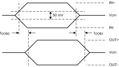
The SN75LVPE802 receiver incorporates an Out-Of-Band (OOB) detection circuit in addition to the main signal chain receiver. The OOB detector continuously monitors the differential input signal to the device. The OOB detector has a 50-mVpp entry threshold. If the differential signal at the receiver input is less than the OOB entry threshold, the device transmitter transitions to squelch. The SN75LVPE802 enters squelch within 5 ns of the input signal falling below the OOB entry threshold. The SN75LVPE802 continues to monitor the input signal while in squelch. While in squelch, if the OOB detector determines that the input signal now exceeds the 90 mVpp exit threshold, the SN75LVPE802 exits squelch within 5 ns.
 Figure 23. OOB Enter and Exit Timing Receiver Input Termination Is Disabled
When the SN75LVPE802 enters squelch state the transmitter output is squelched. The transmitter non-inverting (TX+) output and the transmitter inverting output (TX-) are both driven to the transmitter nominal common mode voltage which is 1.7 V.
8.3.6 Auto Low Power
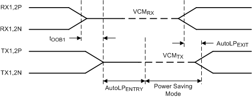
The SN75LVPE801 also includes an Auto Low Power Mode (ALP). ALP is entered when the differential input signal has been less than 50 mV for > 10 µs. The device enters and exits Low Power Mode by actively monitoring the input signal level. In this state the device selectively shuts off internal circuitry to lower power by > 90% of its normal operating power. While in ALP mode the device continues to actively monitor input signal levels. When the input signal exceeds the OOB exit threshold level, the device reverts to the active state. Exit time from Auto Low Power Mode is < 50 ns (max).
 Figure 24. Auto Low Power Mode Entry and Exit Timing
8.3.7 Transmitter Output Signal
The SN75LVPE802 differential output signal is 650 mVpp when de-emphasis is disabled (DE input is open or pulled low).
8.3.8 Transmitter Common Mode
The SN75LVPE802 transmitter common mode output is set to 1.7 V.
8.3.9 De-Emphasis
The SN75LVPE802 device provides the de-emphasis settings shown in Table 2. De-emphasis control is independent for each channel, controlled by the DE1 and DE2 pin settings as shown in Table 2. The reference for the de-emphasis settings available in the device is the transition bit amplitude for each given configuration; this transition bit amplitude is different at 0 dB than the –2-dB and –4-dB settings by design. DEW1 and DEW2 control the DE durations for channels one and two, respectively. Table 2 lists the recommended settings for these control pins. Output de-emphasis is capable of supporting FR4 trace at the output anywhere from 2 in. (5.1 cm) to 12 in. (30.5 cm) at SATA 3G/6G speed.
Table 2. TX and Rx EQ and DE Pulse-Duration Settings
| DEW1 OR DEW2 | DEVICE FUNCTION → DE WIDTH FOR CH1/CH2 |
|---|---|
| 0 | De-emphasis pulse duration, short |
| 1 (default) | De-emphasis pulse duration, long |
8.3.10 Transmitter Termination
The SN75LVPE802 transmitter includes integrated terminations. The receiver differential output impedance is nominally 100 Ω, with a ≤ 22% variation.
8.4 Device Functional Modes
8.4.1 Low-Power Mode
There are two low-power modes supported by the SN75LVPE802 device, listed as follows:
- Standby mode (triggered by the EN pin, EN = 0 V)
- The enable (EN) pin controls th low-power mode. Pulling this pin LOW puts the device in standby mode within 2 µs (max). In this mode, the device drives all its active components to their quiescent level, and differential outputs Hi-Z (open). Maximum power dissipation in this mode is 5 mW. Exiting from this mode to normal operation requires a maximum latency of 5 µs.
- Auto low-power mode (triggered when a given channel is in the electrically idle state for more than 100 µs and EN = VCC)
- The device enters and exits low-power mode by actively monitoring the input signal (VIDp-p) level on each of its channels independently. When the input signal on either or both channels is in the electrically idle state, that is, VIDp-p < 50 mV and stays in this state for > 100 µs, the associated channel enters into the low-power state. In this state, output of the associated channel goes to VCM and the device selectively shuts off some circuitry to lower power by > 80% of its normal operating power. Exit time from the auto low-power mode is < 50 ns.