SLES239A November   2008  – December 2016 TAS5352A

PRODUCTION DATA.  

  1. Features
  2. Applications
  3. Description
  4. Revision History
  5. Pin Configuration and Functions
  6. Specifications
    1. 6.1 Absolute Maximum Ratings
    2. 6.2 ESD Ratings
    3. 6.3 Recommended Operating Conditions
    4. 6.4 Thermal Information
    5. 6.5 Electrical Characteristics
    6. 6.6 Audio Specifications (BTL)
    7. 6.7 Audio Specifications (Single-Ended Output)
    8. 6.8 Audio Specifications (PBTL)
    9. 6.9 Typical Characteristics
      1. 6.9.1 BTL Configuration
      2. 6.9.2 SE Configuration
      3. 6.9.3 PBTL Configuration
  7. Detailed Description
    1. 7.1 Overview
    2. 7.2 Functional Block Diagram
    3. 7.3 Feature Description
      1. 7.3.1 System Power-Up and Power-Down Sequence
        1. 7.3.1.1 Powering Up
        2. 7.3.1.2 Powering Down
      2. 7.3.2 Mid Z Sequence Compatibility
      3. 7.3.3 Error Reporting
      4. 7.3.4 Device Protection System
        1. 7.3.4.1 Use of TAS5352A in High-Modulation-Index Capable Systems
        2. 7.3.4.2 Overcurrent (OC) Protection With Current Limiting and Overload Detection
        3. 7.3.4.3 Pin-to-Pin Short-Circuit Protection (PPSC)
        4. 7.3.4.4 Overtemperature Protection
        5. 7.3.4.5 Undervoltage Protection (UVP) and Power-On-Reset (POR)
      5. 7.3.5 Device Reset
    4. 7.4 Device Functional Modes
      1. 7.4.1 Protection MODE Selection Pins
  8. Application and Implementation
    1. 8.1 Application Information
    2. 8.2 Typical Applications
      1. 8.2.1 BTL Application With AD Modulation Filters - 2N
        1. 8.2.1.1 Design Requirements
        2. 8.2.1.2 Detailed Design Procedure
          1. 8.2.1.2.1 PCB Material Recommendation
          2. 8.2.1.2.2 PVDD Capacitor Recommendation
          3. 8.2.1.2.3 Decoupling Capacitor Recommendations
        3. 8.2.1.3 Application Curves
      2. 8.2.2 BTL Application With AD Modulation Filters - 1N
        1. 8.2.2.1 Design Requirements
      3. 8.2.3 SE Application
        1. 8.2.3.1 Design Requirements
        2. 8.2.3.2 Application Curves
      4. 8.2.4 PBTL Application With AD Modulation Filters
        1. 8.2.4.1 Design Requirements
        2. 8.2.4.2 Application Curves
      5. 8.2.5 Non-Differential PBTL Application
        1. 8.2.5.1 Design Requirements
    3. 8.3 System Example
  9. Power Supply Recommendations
  10. 10Layout
    1. 10.1 Layout Guidelines
    2. 10.2 Layout Example
  11. 11Device and Documentation Support
    1. 11.1 Device Support
      1. 11.1.1 Development Support
    2. 11.2 Documentation Support
      1. 11.2.1 Related Documentation
    3. 11.3 Receiving Notification of Documentation Updates
    4. 11.4 Community Resources
    5. 11.5 Trademarks
    6. 11.6 Electrostatic Discharge Caution
    7. 11.7 Glossary
  12. 12Mechanical, Packaging, and Orderable Information

Package Options

Mechanical Data (Package|Pins)
Thermal pad, mechanical data (Package|Pins)
Orderable Information

Features

  • Total Power Output (Bridge-Tied Load)
    • 2 × 125 W at 10% THD+N Into 4 Ω
    • 2 × 100 W at 10% THD+N Into 6 Ω
  • Total Power Output (Single-Ended)
    • 4 × 45 W at 10% THD+N Into 3 Ω
    • 4 × 35 W at 10% THD+N Into 4 Ω
  • Total Power Output (Parallel Mode)
    • 1 × 250 W at 10% THD+N Into 2 Ω
    • 1 × 195 W at 10% THD+N Into 3 Ω
  • >110 dB SNR (A-Weighted With TAS5518 Modulator)
  • <0.1% THD+N (1 W, 1 kHz)
  • Supports PWM Frame Rates of 192 kHz to
    432 kHz
  • Resistor-Programmable Current Limit
  • Integrated Self-Protection Circuitry, Including:
    • Undervoltage Protection
    • Overtemperature Warning and Error
    • Overload Protection
    • Short-Circuit Protection
    • PWM Activity Detector
  • Stand-Alone Protection Recovery
  • Power-On-Reset (POR) to Eliminate System Power-Supply Sequencing
  • High-Efficiency Power Stage (>90%) With 80-mΩ Output MOSFETs
  • Thermally Enhanced 44-Pin HTSSOP Package (DDV)
  • Error Reporting, 3.3-V and 5-V Compliant
  • EMI Compliant When Used With Recommended System Design

Applications

  • Mini and Micro Audio Systems
  • DVD Receivers
  • Home Theaters

Description

The TAS5352A device is a high-performance, integrated stereo digital amplifier power stage designed to drive a 4-Ω bridge-tied load (BTL) at up to 125 W per channel with low harmonic distortion, low integrated noise, and low idle current.

The TAS5352A has a complete protection system integrated on-chip, safeguarding the device against a wide range of fault conditions that could damage the system. These protection features are short-circuit protection, overcurrent protection, undervoltage protection, overtemperature protection, and a loss of PWM signal (PWM activity detector).

A power-on-reset (POR) circuit is used to eliminate power-supply sequencing that is required for most power-stage designs.

Device Information(1)

PART NUMBER PACKAGE BODY SIZE (NOM)
TAS5352A HTSSOP (44) 14.00 mm × 6.10 mm
  1. For all available packages, see the orderable addendum at the end of the data sheet.

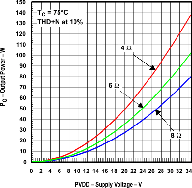
BTL Output Power vs Supply Voltage
TAS5352A gr2_les204_jh2_fp.gif