SLOS814D March   2014  – September 2016 TAS5421-Q1

PRODUCTION DATA.  

  1. Features
  2. Applications
  3. Description
  4. Revision History
  5. Pin Configuration and Functions
  6. Specifications
    1. 6.1 Absolute Maximum Ratings
    2. 6.2 ESD Ratings
    3. 6.3 Recommended Operating Conditions
    4. 6.4 Thermal Information
    5. 6.5 Electrical Characteristics
    6. 6.6 Timing Requirements for I2C Interface Signals
    7. 6.7 Typical Characteristics
  7. Detailed Description
    1. 7.1 Overview
    2. 7.2 Functional Block Diagram
    3. 7.3 Feature Description
      1. 7.3.1 Analog Audio Input and Preamplifier
      2. 7.3.2 Pulse-Width Modulator (PWM)
      3. 7.3.3 Gate Drive
      4. 7.3.4 Power FETs
      5. 7.3.5 Load Diagnostics
      6. 7.3.6 Protection and Monitoring
      7. 7.3.7 I2C Serial Communication Bus
        1. 7.3.7.1 I2C Bus Protocol
        2. 7.3.7.2 Random Write
        3. 7.3.7.3 Random Read
        4. 7.3.7.4 Sequential Read
    4. 7.4 Device Functional Modes
      1. 7.4.1 Hardware Control Pins
      2. 7.4.2 EMI Considerations
      3. 7.4.3 Operating Modes and Faults
    5. 7.5 Register Maps
      1. 7.5.1 I2C Address Register Definitions
  8. Application and Implementation
    1. 8.1 Application Information
    2. 8.2 Typical Application
      1. 8.2.1 Design Requirements
        1. 8.2.1.1 Amplifier Output Filtering
        2. 8.2.1.2 Amplifier Output Snubbers
        3. 8.2.1.3 Bootstrap Capacitors
        4. 8.2.1.4 Analog Audio Input Filter
      2. 8.2.2 Detailed Design Procedure
        1. 8.2.2.1 Unused Pin Connections
          1. 8.2.2.1.1 MUTE Pin
          2. 8.2.2.1.2 STANDBY Pin
          3. 8.2.2.1.3 I2C Pins (SDA and SCL)
          4. 8.2.2.1.4 Terminating Unused Outputs
          5. 8.2.2.1.5 Using a Single-Ended Audio Input
      3. 8.2.3 Application Curves
  9. Power Supply Recommendations
  10. 10Layout
    1. 10.1 Layout Guidelines
    2. 10.2 Layout Examples
      1. 10.2.1 Top Layer
      2. 10.2.2 Second Layer - Signal Layer
      3. 10.2.3 Third Layer - Power Layer
      4. 10.2.4 Bottom Layer - Ground Layer
  11. 11Device and Documentation Support
    1. 11.1 Device Support
      1. 11.1.1 Third-Party Products Disclaimer
    2. 11.2 Documentation Support
      1. 11.2.1 Related Documentation
    3. 11.3 Receiving Notification of Documentation Updates
    4. 11.4 Community Resource
    5. 11.5 Trademarks
    6. 11.6 Electrostatic Discharge Caution
    7. 11.7 Glossary
  12. 12Mechanical, Packaging, and Orderable Information

Package Options

Mechanical Data (Package|Pins)
Thermal pad, mechanical data (Package|Pins)
Orderable Information

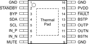
5 Pin Configuration and Functions

PWP Package
16-Pin TSSOP With Exposed Thermal Pad
Top View
TAS5421-Q1 Pinout_SLOS814.gif

Pin Functions

PIN TYPE(1) DESCRIPTION
NAME NO.
BSTN 10 AI Bootstrap for negative-output high-side FET
BSTP 13 AI Bootstrap for positive-output high-side FET
BYP 3 PBY Voltage-regulator bypass-capacitor pin
FAULT 14 DO Active-low open-drain output used to report faults
GND 1 GND Ground
9
16
IN_N 7 AI Inverting analog input
IN_P 6 AI Non-inverting analog input
MUTE 8 DI Mute input, active-high (no internal pullup or pulldown)
OUTN 11 PO Output (–)
OUTP 12 PO Output (+)
PVDD 15 PWR Power supply
SCL 5 DI I2C clock
SDA 4 DI/DO I2C data
STANDBY 2 DI Active-low STANDBY pin (no internal pullup or pulldown)
Thermal pad Must be soldered to ground
(1) DI = digital input, DO = digital output, AI = analog input, PWR = power supply, PBY = power bypass, PO = power output, GND = ground