SLOS814D March 2014 – September 2016 TAS5421-Q1
PRODUCTION DATA.
- 1 Features
- 2 Applications
- 3 Description
- 4 Revision History
- 5 Pin Configuration and Functions
- 6 Specifications
- 7 Detailed Description
- 8 Application and Implementation
- 9 Power Supply Recommendations
- 10Layout
- 11Device and Documentation Support
- 12Mechanical, Packaging, and Orderable Information
Package Options
Mechanical Data (Package|Pins)
- PWP|16
Thermal pad, mechanical data (Package|Pins)
- PWP|16
Orderable Information
6 Specifications
6.1 Absolute Maximum Ratings
over operating free-air temperature range (unless otherwise noted) (1)| MIN | MAX | UNIT | |||
|---|---|---|---|---|---|
| Input voltage | DC supply voltage range, V(PVDD) | Relative to GND | –0.3 | 30 | V |
| Pulsed supply voltage range, V(PVDD_MAX) | t ≤ 400 ms exposure | –1 | 40 | ||
| Supply voltage ramp rate, ΔV(PVDD_RAMP) | 15 | V/ms | |||
| For SCL, SDA, and STANDBY pins | Relative to GND | –0.3 | 5 | V | |
| For IN_N, IN_P, FAULT, and MUTE pins | Relative to GND | –0.3 | 6.5 | ||
| Current | DC current on PVDD, GND and OUTx pins, I(PVDD), IO | ±4 | A | ||
| Maximum current, on all input pins, I(IN_MAX) (2) | ±1 | mA | |||
| Maximum sink current for open-drain pin, I(IN_ODMAX) | 7 | ||||
| Storage temperature, Tstg | –55 | 150 | °C | ||
(1) Stresses beyond those listed under Absolute Maximum Ratings may cause permanent damage to the device. These are stress ratings only, which do not imply functional operation of the device at these or any other conditions beyond those indicated under Recommended Operating Conditions. Exposure to absolute-maximum-rated conditions for extended periods may affect device reliability.
(2) See the Application and Implementation section for information on analog input voltage and ac coupling.
6.2 ESD Ratings
| VALUE | UNIT | ||||
|---|---|---|---|---|---|
| V(ESD) | Electrostatic discharge | Human-body model (HBM), per AEC Q100-002(1) | ±3500 | V | |
| Charged-device model (CDM), per AEC Q100-011 | ±1000 | ||||
(1) AEC Q100-002 indicates that HBM stressing shall be in accordance with the ANSI/ESDA/JEDEC JS-001 specification.
6.3 Recommended Operating Conditions
| MIN | NOM | MAX | UNIT | |||
|---|---|---|---|---|---|---|
| V(PVDD_OP) | Supply voltage range relative to GND. Includes ac transients, requires proper decoupling.(3) | 4-Ω ±20% load (or higher) |
4.5 | 14.4 | 18 | V |
| 2-Ω ±20% load | 5 | 14.4 | 18 | |||
| V(PVDD_RIPPLE) | Maximum ripple on PVDD | V(PVDD) < 8 V | 1 | Vpp | ||
| V(AIN)(1) | Analog audio input-signal level | AC-coupled input voltage | 0 | 0.25–1(2) | Vrms | |
| V(IH_STANDBY) | MUTE and STANDBY pins input voltage for logic-level high | 2 | V | |||
| V(IL_STANDBY) | MUTE and STANDBY pins input voltage for logic-level low | 0.7 | V | |||
| V(IH_SCL) | SCL pin input voltage for logic-level high | R(PU_I2C) = 4.7-kΩ pullup, supply voltage = 3.3 V or 5 V | 2.1 | 5.5 | V | |
| V(IH_SDA) | SDA pin input voltage for logic-level high | R(PU_I2C) = 4.7-kΩ pullup, supply voltage = 3.3 V or 5 V | 2.1 | 5.5 | V | |
| V(IL_SCL) | SCL pin input voltage for logic-level low | R(PU_I2C) = 4.7-kΩ pullup, supply voltage = 3.3 V or 5 V | –0.5 | 1.1 | V | |
| V(IL_SDA) | SDA pin input voltage for logic-level low | R(PU_I2C) = 4.7-kΩ pullup, supply voltage = 3.3 V or 5 V | –0.5 | 1.1 | V | |
| TA | Ambient temperature | –40 | 125 | °C | ||
| R(L) | Nominal speaker load impedance | When using low-impedance loads, do not exceed overcurrent limit. | 2 | 4 | 16 | Ω |
| V(PU) | Pullup voltage supply (for open-drain logic outputs) | 3 | 3.3 | 3.6 | V | |
| R(PU_EXT) | External pullup resistor on open-drain logic outputs | Resistor connected between open-drain logic output and V(PU) supply. | 10 | 50 | kΩ | |
| R(PU_I2C) | I2C pullup resistance on SDA and SCL pins | 1 | 4.7 | 10 | kΩ | |
| C(PVDD) | External capacitor on the PVDD pin, typical value ± 20%(3) | 10 | μF | |||
| C(BYP) | External capacitor on the BYP pin, typical value ± 10% | 1 | μF | |||
| C(OUT) | External capacitance to GND on OUT_X pins | 4 | μF | |||
| C(IN) | External capacitance to analog input pin in series with input signal | 1 | μF | |||
| C(BSTN), C(BSTP) | External boostrap capacitor, typical value ± 20% | 220 | nF | |||
(1) Signal input for full unclipped output with gains of 36 dB, 32 dB, 26 dB, and 20 dB
(2) Maximum recommended input voltage is determined by the gain setting.
(3) See the Power Supply Recommendations section.
6.4 Thermal Information
| THERMAL METRIC(1) | TAS5421-Q1 | UNIT | |
|---|---|---|---|
| PWP (HTSSOP) | |||
| 16 PINS | |||
| RθJA | Junction-to-ambient thermal resistance | 39.4 | °C/W |
| RθJC(top) | Junction-to-case (top) thermal resistance | 24.9 | °C/W |
| RθJB | Junction-to-board thermal resistance | 20 | °C/W |
| ψJT | Junction-to-top characterization parameter | 0.6 | °C/W |
| ψJB | Junction-to-board characterization parameter | 19.8 | °C/W |
| RθJC(bot) | Junction-to-case (bottom) thermal resistance | 2 | °C/W |
(1) For more information about traditional and new thermal metrics, see the Semiconductor and IC Package Thermal Metrics application report.
6.5 Electrical Characteristics
TC = 25°C, PVDD = 14.4 V, RL = 4 Ω, P(O) = 1 W/ch, AES17 filter, default I2C settings (unless otherwise noted)6.6 Timing Requirements for I2C Interface Signals
over recommended operating conditions (unless otherwise noted)| MIN | NOM | MAX | UNIT | ||
|---|---|---|---|---|---|
| f(SCL) | SCL clock frequency | 400 | kHz | ||
| tr | Rise time for both SDA and SCL signals | 300 | ns | ||
| tf | Fall time for both SDA and SCL signals | 300 | ns | ||
| tw(H) | SCL pulse duration, high | 0.6 | µs | ||
| tw(L) | SCL pulse duration, low | 1.3 | µs | ||
| tsu(2) | Setup time for START condition | 0.6 | µs | ||
| th(2) | START condition hold time before generation of first clock pulse | 0.6 | µs | ||
| tsu(1) | Data setup time | 100 | ns | ||
| th(1) | Data hold time | 0(1) | ns | ||
| tsu(3) | Setup time for STOP condition | 0.6 | µs | ||
| C(B) | Load capacitance for each bus line | 400 | pF | ||
(1) A device must internally provide a hold time of at least 300 ns for the SDA signal to bridge the undefined region of the falling edge of SCL.
 Figure 1. SCL and SDA Timing
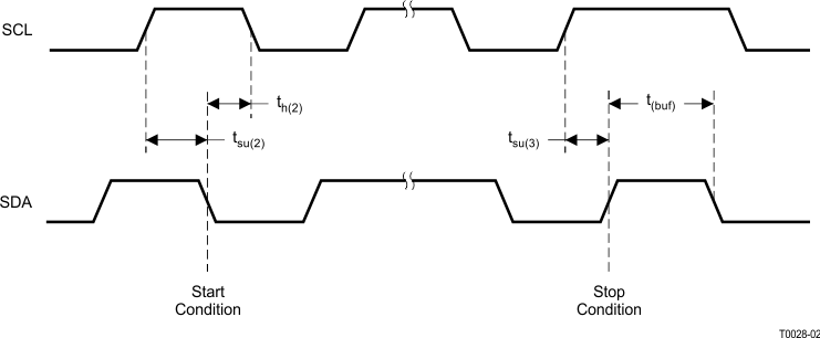 Figure 2. Timing for Start and Stop Conditions
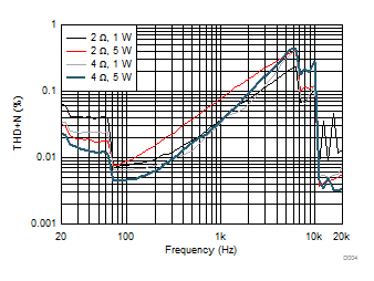
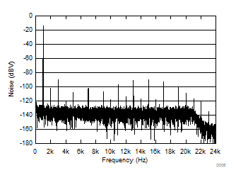
6.7 Typical Characteristics
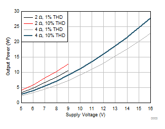
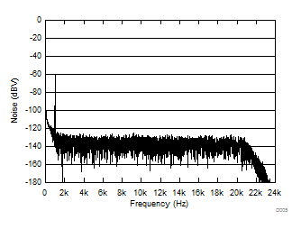
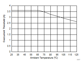
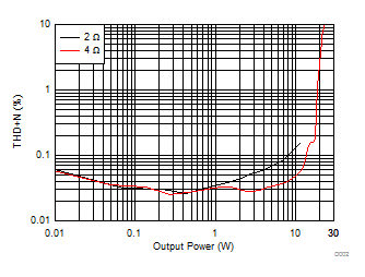
PVDD = 14.4 V, TA = 25ºC, P(O) = 1 W, 1-kHz input, default I2C settings (unless otherwise noted)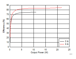
| Gain = 26 dB | f(SW) = 400 kHz | TA = 25ºC |
| V(PVDD) = 14.4 V |
