SLES273B April 2013 – April 2015 TAS5558
PRODUCTION DATA.
- 1 Features
- 2 Applications
- 3 Description
- 4 Revision History
- 5 Pin Configuration and Functions
-
6 Specifications
- 6.1 Absolute Maximum Ratings
- 6.2 ESD Ratings
- 6.3 Recommended Operating Conditions
- 6.4 Thermal Information
- 6.5 Electrical Characteristics
- 6.6 Dynamic Performance
- 6.7 SRC Performance
- 6.8 Timing I2C Serial Control Port Operation
- 6.9 Reset Timing (RESET)
- 6.10 Power-Down (PDN) Timing
- 6.11 Back-End Error (BKND_ERR)
- 6.12 Mute Timing (MUTE)
- 6.13 Headphone Select (HP_SEL)
- 6.14 Switching Characteristics - Clock Signals
- 6.15 Switching Characteristics - Serial Audio Port
- 6.16 Volume Control
- 6.17 Typical Characteristics
-
7 Detailed Description
- 7.1 Overview
- 7.2 Functional Block Diagram
- 7.3 Feature Description
- 7.4
Device Functional Modes
- 7.4.1 Power Supply
- 7.4.2 Clock, PLL, and Serial Data Interface
- 7.4.3 Serial Audio Interface
- 7.4.4 I 2C Serial-Control Interface
- 7.4.5 Device Control
- 7.4.6 Energy Manager
- 7.4.7 Digital Audio Processor (DAP)
- 7.4.8 Pulse Width Modulation Schemes
- 7.4.9 TAS5558 DAP Architecture Diagrams
- 7.4.10 I 2C Coefficient Number Formats
- 7.4.11 Input Crossbar Mixer
- 7.4.12 Biquad Filters
- 7.4.13 Bass and Treble Controls
- 7.4.14 Volume, Automute, and Mute
- 7.4.15 Loudness Compensation
- 7.4.16 Dynamic Range Control (DRC)
- 7.4.17 THD Manager
- 7.4.18 Downmix Algorithm and I2S Out
- 7.4.19 Stereo Downmixes/(or Fold-Downs)
- 7.4.20 Output Mixer
- 7.4.21 Device Configuration Controls
- 7.4.22 Master Clock and Serial Data Rate Controls
- 7.4.23 Bank Controls (ASRC Bypass only)
- 7.5 Programming
- 7.6
Register Maps
- 7.6.1 Serial-Control I2C Register Summary
- 7.6.2
Serial-Control Interface Register Definitions
- 7.6.2.1 Clock Control Register (0x00)
- 7.6.2.2 General Status Register 0 (0x01)
- 7.6.2.3 Error Status Register (0x02)
- 7.6.2.4 System Control Register 1 (0x03)
- 7.6.2.5 System Control Register 2 (0x04)
- 7.6.2.6 Channel Configuration Control Registers (0x05-0x0C)
- 7.6.2.7 Headphone Configuration Control Register (0x0D)
- 7.6.2.8 Serial Data Interface Control Register (0x0E)
- 7.6.2.9 Soft Mute Register (0x0F)
- 7.6.2.10 Energy Manager Status Register (0x10)
- 7.6.2.11 Automute Control Register (0x14)
- 7.6.2.12 Output Automute PWM Threshold and Back-End Reset Period Register (0x15)
- 7.6.2.13 Modulation Index Limit Register (0x16, 0x17, 0x18, 0x19)
- 7.6.2.14 AD Mode - 8 Interchannel Channel Delay and Global Offset Registers (0x1B to 0x23)
- 7.6.2.15 Special Low Z and Mid Z Ramp/Stop Period (0x24)
- 7.6.2.16 PWM and EMO Control Register (0x25)
- 7.6.2.17 Individual Channel Shutdown (0x27)
- 7.6.2.18 Input Mux Registers (0x30, 0x31, 0x32, 0x33)
- 7.6.2.19 PWM Mux Registers (0x34, 0x35, 0x36, 0x37)
- 7.6.2.20 BD Mode and Ternary - 8 Interchannel Channel Delay (0x38 to 0x3F)
- 7.6.2.21 Bank-Switching Command Register (0x40) (TAS5558 + ASRC Bypass)
- 7.6.2.22 Input Mixer Registers, Channels 1-8 (0x41-0x48)
- 7.6.2.23 Bass Mixer Registers (0x49-0x50)
- 7.6.2.24 Biquad Filter Register (0x51-0x88)
- 7.6.2.25 Bass and Treble Register, Channels 1-8 (0x89-0x90)
- 7.6.2.26 Loudness Registers (0x91-0x95)
- 7.6.2.27 DRC1 Control Register CH1-7 (0x96) - Write
- 7.6.2.28 DRC2 Control Register CH8 (0x97) - Write Register
- 7.6.2.29 DRC1 Data Registers (0x98-0x9C)
- 7.6.2.30 DRC2 Data Registers (0x9D-0xA1)
- 7.6.2.31 DRC Bypass Registers (0xA2-0xA9)
- 7.6.2.32 Output Select and Mix Registers 8x2 (0x-0xAF)
- 7.6.2.33 8×3 Output Mixer Registers (0xB0-0xB1)
- 7.6.2.34 ASRC Registers (0xC3-C5)
- 7.6.2.35 Auto Mute Behavior (0xCC)
- 7.6.2.36 PSVC Volume Biquad Register (0xCF)
- 7.6.2.37 Volume, Treble, and Bass Slew Rates Register (0xD0)
- 7.6.2.38 Volume Registers (0xD1-0xD9)
- 7.6.2.39 Bass Filter Set Register (0xDA)
- 7.6.2.40 Bass Filter Index Register (0xDB)
- 7.6.2.41 Treble Filter Set Register (0xDC)
- 7.6.2.42 Treble Filter Index (0xDD)
- 7.6.2.43 AM Mode Register (0xDE)
- 7.6.2.44 PSVC Range Register (0xDF)
- 7.6.2.45 General Control Register (0xE0)
- 7.6.2.46 96kHz Dolby Downmix Coefficients (0xE3 to 0xE8)
- 7.6.2.47 THD Manager Configuration (0xE9 and 0xEA)
- 7.6.2.48 SDIN5 Input Mixer (0xEC-0xF3)
- 7.6.2.49 192kHZ Process Flow Output Mixer (0xF4-0xF7)
- 7.6.2.50 192kHz Dolby Downmix Coefficients (0xFB and 0xFC)
- 8 Application and Implementation
- 9 Power Supply Recommendations
- 10Layout
- 11Device and Documentation Support
- 12Mechanical, Packaging, and Orderable Information
Package Options
Mechanical Data (Package|Pins)
- DCA|56
Thermal pad, mechanical data (Package|Pins)
- DCA|56
Orderable Information
8 Application and Implementation
NOTE
Information in the following applications sections is not part of the TI component specification, and TI does not warrant its accuracy or completeness. TI’s customers are responsible for determining suitability of components for their purposes. Customers should validate and test their design implementation to confirm system functionality.
8.1 Application Information
The TAS5558 is a PWM modulator that can take in up to 10 serial audio channels with 8 fully-differential PWM outputs, 2 fully-differential headphone PWM outputs, and up to 1 serial audio output. The eight PWM outputs can support single-ended or bridge-tied load-configured H-bridge power stages with either AD or BD modulation. The 10 inputs can be mixed and mapped internally to different outputs. The TAS5558 is designed to seamlessly interface with most digital decoders, and supports the DTS-HD specification and Blu-ray HTiB applications.
The TAS5558 also contains a DAP that can implement up to 56 biquads across the 8 channels for sampling rates up to 96-kHz, and 22 for sampling rates above 96-kHz. Two 4-channel sample rate converters process the inputs before passing the signals to the DAP. The TAS5558 can be driven by an external crystal or an external MCLK. Two 3.3-V power supplies are required for a digital and analog supply.
8.2 Typical Applications
Typical applications for the TAS5558 are 6- to 8-channel audio systems such as DVD or AV receivers. Figure 45 shows the basic system diagram of the DVD receiver.
8.2.1 TAS5558 DVD Receiver Application
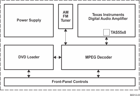 Figure 45. Typical TAS5558 Application (DVD Receiver)
8.2.1.1 Design Requirements
For this design example, use the parameters listed in Table 87 as the input parameters.
Table 87. Design Parameters
| PARAMETER | VALUE |
|---|---|
| Device control method | Software control through I2C communication for register settings |
| Digital Audio input | Right-justified, I2S, or left-justified. |
| Power stage | Audio amplifier with PWM input |
8.2.1.2 Detailed Design Procedure
- System software control over I2C for part configuration on power up
- I2S sample rate and number of channels
- If the sampling rate above 96-kHz, then the number of biquads is limited.
- Tuning of biquad filters to preferred settings
- Possible headphone out that would require an output filter
- Use of the TAS5558 Frequency Scaling AM Avoidance to prevent interference with AM tuner
8.2.1.3 Application Curves
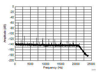
8.2.2 Serial Port Master/Slave Configurations
The inputs to the Digital Audio Processor (DAP) come from the Asynchronous Sample Rate Converter block as follows:
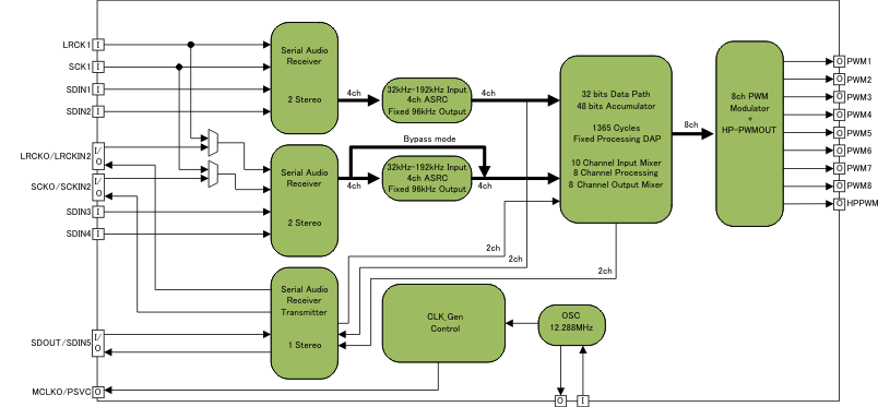 Figure 47. Digital Audio Signal Flow Block Diagram
8.2.2.1 Design Requirements
For this design example, use the parameters listed in Table 88 as the input parameters.
Table 88. Design Parameters
| PARAMETER | VALUE |
|---|---|
| Device control method | Software control through I2C communication for register settings |
| Digital Audio input | Right-justified, I2S, or left-justified. |
| Power stage | Audio amplifier with PWM input |
8.2.2.2 Detailed Design Procedure
The DAP can feed audio data to and from the Serial Audio ports in the following manner. There are 3 main use cases:
-
Use Case 1: External Karaoke Microphone Input (ADC in on SDIN5) or External I2S Subwoofer
- SDIN1 through 4 are slave to an external source (such as a media decoder IC).
- A separate DOUT (for Sub) or Microphone Inout (SDIN5) needs to function at the post-ASRC rate.
- Therefore, the device is configured to use MCLKO, SCLKO and LRCLKO.
-
Use Case 2: Mixing two different data sources (e.g. Stereo Bluetooth I2S and CD/Media Decoder
- In an example where two different data sources need mixing, SDIN1/2 run at a different rate than SDIN3/4
- SCLKIN-2 and LRCLKIN-2 are used to provide an LRCLK and SCLK for the second data synchronous data source.
- DOUT (for a wireless sub) cannot be used in this mode, as no MCLKO, SCLKO or LRCLKO are available.
-
Use Case 3: Creating an external loop for processing (e.g. using a TAS3108 or TAS3152 I2S processor)
- SDIN1/2 run with SCLK and LRCLK as a slave.
- SDOUT acts as a "send for external processing", in master mode, synchronized to MLCKO, SCLKO, LRCLKO
- SDIN3/4 Act as a "return from external processing", in master mode, synchronized to MLCKO, SCLKO, LRCLKO
Table 89. Master/Slave Serial Audio Receiver/Transmitter
| Slave Serial Audio port | Master Serial Audio port | |
|---|---|---|
| Use case-1 |
|
|
| Use case-2 |
|
None of Master |
| Use case-3 |
|
|
By using use case-3, TAS5558 can connect TAS3108 as external co-processor as follows:
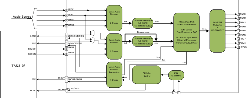 Figure 48. TAS3108 as External Co-processor
8.2.2.3 Application Curves

8.2.3 Device System Diagrams
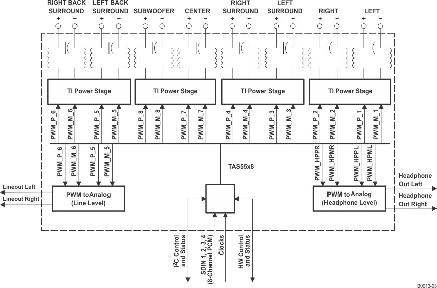 Figure 50. Pass-Through Output Mixer TAS5558 Channel Configuration
8.2.3.1 Design Requirements
- Device control method: Software control through I2C communication for register settings
- Digital Audio input: right-justified, I2S, or left-justified at 96kHz or below to enable use of all 8 channels and related biquads
- Power stage: Audio amplifier with PWM input
- Clock Source: External clocks from I2S master
8.2.3.2 Detailed Design Procedure
- System software control over I2C for part configuration on power up
- I2S sample rate and number of channels
- If the sampling rate is above 96-kHz, then the number of biquads is limited.
- Tuning of biquad filters to preferred settings
- Possible headphone out that would require an output filter
- Choose the appropriate LC output filters after power stage for speaker load
8.2.3.3 Application Curves

8.3 Do’s and Don’ts
8.3.1 Frequency Scaling AM Avoidance
The AM avoidance strategy exploits the presence of the ASRC. The APLL output frequency is directly varied by varying the multiplier ratio in the PLL loop. The dividers to generate clocks from the APLL are fixed at their nominal division factor, so the result is that the internal sampling rate is changing accordingly.
The ASRC will adapt with this changing output rate (the internal sampling rate) and convert the incoming sampling rates to this rate accordingly. The rest of the circuit does not change and operates normally, but since the APLL output frequency is varied while the clock dividers are fixed, the PWM carrier frequency becomes varied also, which is the goal of this AM avoidance strategy.
This shift in processing rate will effect time-domain digital processing, such as the EQ's and DRC's decay values by the value in Freq_Error below.
Table 90. APLL/DAP/ASRC Clock Frequencies with New AM Avoidance Strategy
| Mode | Input FS | MCLK | Prescale | Feedback | DCLK | Internal SR | DAP CLK | # cycles per FS | ASRC CLK | PWM rate | Freq_Error |
|---|---|---|---|---|---|---|---|---|---|---|---|
| Normal | 8 - 192k | 12288 | 4 | 64 | 196608 | 96 | 131072 | 1365.33 | 98304 | 384 | 0.00% |
| AM#1 | 8 - 192k | 12288 | 4 | 62 | 190464 | 93 | 126976 | 1365.33 | 95232 | 372 | -3.13% |
| AM#2 | 8 - 192k | 12288 | 4 | 60 | 184320 | 90 | 12288 | 1365.33 | 92160 | 360 | -6.25% |
| AM#3 | 8 - 192k | 12288 | 4 | 58 | 178176 | 87 | 118784 | 1365.33 | 89088 | 348 | -9.38% |
| AM#4 | 8 - 192k | 12288 | 4 | 56 | 172032 | 84 | 114688 | 1365.33 | 86016 | 336 | -12.50% |
8.4 Initialization Set Up
8.4.1 Startup Register Writes to get Audio Functioning
By default, the device starts up with its outputs muted. The following writes should be used to bring it out of standby:
TAS5558
- Trim Register 0x12 = 00 (selects the internal factory trim)
- Exit Shutdown 0x03 = A0
- Set Master Volume 0xD9 = 00 00 00 48