SLES273B April   2013  – April 2015 TAS5558

PRODUCTION DATA.  

  1. Features
  2. Applications
  3. Description
  4. Revision History
  5. Pin Configuration and Functions
  6. Specifications
    1. 6.1  Absolute Maximum Ratings
    2. 6.2  ESD Ratings
    3. 6.3  Recommended Operating Conditions
    4. 6.4  Thermal Information
    5. 6.5  Electrical Characteristics
    6. 6.6  Dynamic Performance
    7. 6.7  SRC Performance
    8. 6.8  Timing I2C Serial Control Port Operation
    9. 6.9  Reset Timing (RESET)
    10. 6.10 Power-Down (PDN) Timing
    11. 6.11 Back-End Error (BKND_ERR)
    12. 6.12 Mute Timing (MUTE)
    13. 6.13 Headphone Select (HP_SEL)
    14. 6.14 Switching Characteristics - Clock Signals
    15. 6.15 Switching Characteristics - Serial Audio Port
    16. 6.16 Volume Control
    17. 6.17 Typical Characteristics
  7. Detailed Description
    1. 7.1 Overview
    2. 7.2 Functional Block Diagram
    3. 7.3 Feature Description
      1. 7.3.1 Serial Audio Interface Control and Timing
        1. 7.3.1.1 Input I2S Timing
        2. 7.3.1.2 Left-Justified Timing
        3. 7.3.1.3 Right-Justified Timing
      2. 7.3.2 OUTPUT Serial Audio Output
      3. 7.3.3 I2S Master Mode
      4. 7.3.4 LRCKO and SCLKO
      5. 7.3.5 PWM Features
        1. 7.3.5.1 DC Blocking (High-Pass Filter Enable/Disable)
        2. 7.3.5.2 AM Interference Avoidance
      6. 7.3.6 TAS5558 Controls and Status
        1. 7.3.6.1 I2C Status Registers
          1. 7.3.6.1.1 General Status Register (0x01)
          2. 7.3.6.1.2 Error Status Register (0x02)
        2. 7.3.6.2 TAS5558 Pin Controls
          1. 7.3.6.2.1 Reset (RESET)
          2. 7.3.6.2.2 Power Down (PDN)
          3. 7.3.6.2.3 Back-End Error (BKND_ERR)
            1. 7.3.6.2.3.1 BKND_ERR and VALID
          4. 7.3.6.2.4 Speaker/Headphone Selector (HP_SEL)
          5. 7.3.6.2.5 Mute (MUTE)
          6. 7.3.6.2.6 Power-Supply Volume Control (PSVC)
    4. 7.4 Device Functional Modes
      1. 7.4.1  Power Supply
      2. 7.4.2  Clock, PLL, and Serial Data Interface
      3. 7.4.3  Serial Audio Interface
      4. 7.4.4  I 2C Serial-Control Interface
      5. 7.4.5  Device Control
      6. 7.4.6  Energy Manager
      7. 7.4.7  Digital Audio Processor (DAP)
        1. 7.4.7.1 TAS5558 Audio-Processing Configurations
        2. 7.4.7.2 TAS5558 Audio-Processing Feature Sets
      8. 7.4.8  Pulse Width Modulation Schemes
      9. 7.4.9  TAS5558 DAP Architecture Diagrams
      10. 7.4.10 I 2C Coefficient Number Formats
        1. 7.4.10.1 Digital Audio Processor (DAP) Arithmetic Unit
        2. 7.4.10.2 28-Bit 5.23 Number Format
        3. 7.4.10.3 TAS5558 Audio Processing
      11. 7.4.11 Input Crossbar Mixer
      12. 7.4.12 Biquad Filters
      13. 7.4.13 Bass and Treble Controls
      14. 7.4.14 Volume, Automute, and Mute
      15. 7.4.15 Loudness Compensation
        1. 7.4.15.1 Loudness Example
      16. 7.4.16 Dynamic Range Control (DRC)
        1. 7.4.16.1 DRC Implementation
        2. 7.4.16.2 Compression/Expansion Coefficient Computation Engine Parameters
          1. 7.4.16.2.1 Threshold Parameter Computation
          2. 7.4.16.2.2 Offset Parameter Computation
          3. 7.4.16.2.3 Slope Parameter Computation
      17. 7.4.17 THD Manager
      18. 7.4.18 Downmix Algorithm and I2S Out
      19. 7.4.19 Stereo Downmixes/(or Fold-Downs)
        1. 7.4.19.1 Left Total/Right Total (Lt/Rt)
        2. 7.4.19.2 Left Only/Right Only (Lo/Ro)
      20. 7.4.20 Output Mixer
      21. 7.4.21 Device Configuration Controls
        1. 7.4.21.1 Channel Configuration
        2. 7.4.21.2 Headphone Configuration Registers
        3. 7.4.21.3 Audio System Configurations
          1. 7.4.21.3.1 Using Line Outputs in 6-Channel Configurations
        4. 7.4.21.4 Recovery from Clock Error
        5. 7.4.21.5 Power-Supply Volume-Control Enable
        6. 7.4.21.6 Volume and Mute Update Rate
        7. 7.4.21.7 Modulation Index Limit
      22. 7.4.22 Master Clock and Serial Data Rate Controls
        1. 7.4.22.1 192kHz Native Processing Mode
        2. 7.4.22.2 Supported MCLK Frequencies on the TAS5558
        3. 7.4.22.3 PLL Operation
        4. 7.4.22.4 MCLK Ratio Auto Detection
      23. 7.4.23 Bank Controls (ASRC Bypass only)
        1. 7.4.23.1 Manual Bank Selection
        2. 7.4.23.2 Automatic Bank Selection
          1. 7.4.23.2.1 Coefficient Write Operations While Automatic Bank Switch Is Enabled
        3. 7.4.23.3 Bank Set
        4. 7.4.23.4 Bank-Switch Timeline
        5. 7.4.23.5 Bank-Switching Example 1
    5. 7.5 Programming
      1. 7.5.1 I2C Serial-Control Interface (Slave Addresses 0x36)
        1. 7.5.1.1 General I2C Operation
        2. 7.5.1.2 Single- and Multiple-Byte Transfers
        3. 7.5.1.3 Single-Byte Write
        4. 7.5.1.4 Multiple-Byte Write
        5. 7.5.1.5 Incremental Multiple-Byte Write
        6. 7.5.1.6 Single-Byte Read
        7. 7.5.1.7 Multiple-Byte Read
    6. 7.6 Register Maps
      1. 7.6.1 Serial-Control I2C Register Summary
      2. 7.6.2 Serial-Control Interface Register Definitions
        1. 7.6.2.1  Clock Control Register (0x00)
        2. 7.6.2.2  General Status Register 0 (0x01)
        3. 7.6.2.3  Error Status Register (0x02)
        4. 7.6.2.4  System Control Register 1 (0x03)
        5. 7.6.2.5  System Control Register 2 (0x04)
        6. 7.6.2.6  Channel Configuration Control Registers (0x05-0x0C)
        7. 7.6.2.7  Headphone Configuration Control Register (0x0D)
        8. 7.6.2.8  Serial Data Interface Control Register (0x0E)
        9. 7.6.2.9  Soft Mute Register (0x0F)
        10. 7.6.2.10 Energy Manager Status Register (0x10)
        11. 7.6.2.11 Automute Control Register (0x14)
        12. 7.6.2.12 Output Automute PWM Threshold and Back-End Reset Period Register (0x15)
        13. 7.6.2.13 Modulation Index Limit Register (0x16, 0x17, 0x18, 0x19)
        14. 7.6.2.14 AD Mode - 8 Interchannel Channel Delay and Global Offset Registers (0x1B to 0x23)
        15. 7.6.2.15 Special Low Z and Mid Z Ramp/Stop Period (0x24)
        16. 7.6.2.16 PWM and EMO Control Register (0x25)
        17. 7.6.2.17 Individual Channel Shutdown (0x27)
        18. 7.6.2.18 Input Mux Registers (0x30, 0x31, 0x32, 0x33)
        19. 7.6.2.19 PWM Mux Registers (0x34, 0x35, 0x36, 0x37)
        20. 7.6.2.20 BD Mode and Ternary - 8 Interchannel Channel Delay (0x38 to 0x3F)
        21. 7.6.2.21 Bank-Switching Command Register (0x40) (TAS5558 + ASRC Bypass)
        22. 7.6.2.22 Input Mixer Registers, Channels 1-8 (0x41-0x48)
        23. 7.6.2.23 Bass Mixer Registers (0x49-0x50)
        24. 7.6.2.24 Biquad Filter Register (0x51-0x88)
        25. 7.6.2.25 Bass and Treble Register, Channels 1-8 (0x89-0x90)
        26. 7.6.2.26 Loudness Registers (0x91-0x95)
        27. 7.6.2.27 DRC1 Control Register CH1-7 (0x96) - Write
        28. 7.6.2.28 DRC2 Control Register CH8 (0x97) - Write Register
        29. 7.6.2.29 DRC1 Data Registers (0x98-0x9C)
        30. 7.6.2.30 DRC2 Data Registers (0x9D-0xA1)
        31. 7.6.2.31 DRC Bypass Registers (0xA2-0xA9)
        32. 7.6.2.32 Output Select and Mix Registers 8x2 (0x-0xAF)
        33. 7.6.2.33 8×3 Output Mixer Registers (0xB0-0xB1)
        34. 7.6.2.34 ASRC Registers (0xC3-C5)
        35. 7.6.2.35 Auto Mute Behavior (0xCC)
        36. 7.6.2.36 PSVC Volume Biquad Register (0xCF)
        37. 7.6.2.37 Volume, Treble, and Bass Slew Rates Register (0xD0)
        38. 7.6.2.38 Volume Registers (0xD1-0xD9)
        39. 7.6.2.39 Bass Filter Set Register (0xDA)
        40. 7.6.2.40 Bass Filter Index Register (0xDB)
        41. 7.6.2.41 Treble Filter Set Register (0xDC)
        42. 7.6.2.42 Treble Filter Index (0xDD)
        43. 7.6.2.43 AM Mode Register (0xDE)
        44. 7.6.2.44 PSVC Range Register (0xDF)
        45. 7.6.2.45 General Control Register (0xE0)
        46. 7.6.2.46 96kHz Dolby Downmix Coefficients (0xE3 to 0xE8)
        47. 7.6.2.47 THD Manager Configuration (0xE9 and 0xEA)
        48. 7.6.2.48 SDIN5 Input Mixer (0xEC-0xF3)
        49. 7.6.2.49 192kHZ Process Flow Output Mixer (0xF4-0xF7)
        50. 7.6.2.50 192kHz Dolby Downmix Coefficients (0xFB and 0xFC)
  8. Application and Implementation
    1. 8.1 Application Information
    2. 8.2 Typical Applications
      1. 8.2.1 TAS5558 DVD Receiver Application
        1. 8.2.1.1 Design Requirements
        2. 8.2.1.2 Detailed Design Procedure
        3. 8.2.1.3 Application Curves
      2. 8.2.2 Serial Port Master/Slave Configurations
        1. 8.2.2.1 Design Requirements
        2. 8.2.2.2 Detailed Design Procedure
        3. 8.2.2.3 Application Curves
      3. 8.2.3 Device System Diagrams
        1. 8.2.3.1 Design Requirements
        2. 8.2.3.2 Detailed Design Procedure
        3. 8.2.3.3 Application Curves
    3. 8.3 Do’s and Don’ts
      1. 8.3.1 Frequency Scaling AM Avoidance
    4. 8.4 Initialization Set Up
      1. 8.4.1 Startup Register Writes to get Audio Functioning
  9. Power Supply Recommendations
    1. 9.1 Power Supply
    2. 9.2 Energy Manager
    3. 9.3 Programming Energy Manager
  10. 10Layout
    1. 10.1 Layout Guidelines
    2. 10.2 Layout Example
  11. 11Device and Documentation Support
    1. 11.1 Documentation Support
      1. 11.1.1 Related Documentation
    2. 11.2 Trademarks
    3. 11.3 Electrostatic Discharge Caution
    4. 11.4 Glossary
  12. 12Mechanical, Packaging, and Orderable Information

Package Options

Mechanical Data (Package|Pins)
Thermal pad, mechanical data (Package|Pins)
Orderable Information

5 Pin Configuration and Functions

TAS5558 DCA Package
56-Pin HTSSOP
Top View
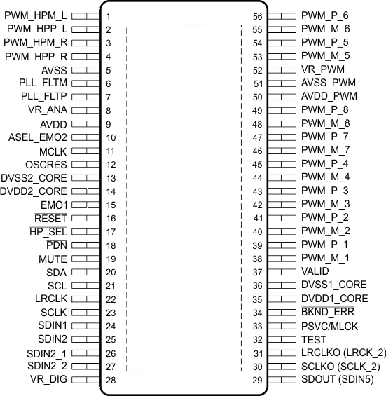
TAS5558 P0113-02_les270.gif

Pin Functions

PIN TYPE 5-V
TOLERANT
TERMINATION DESCRIPTION
NAME NO.
ASEL_EMO2 10 DIO Pullup I2C Address Select. Address will 0X34/0X36 with the value of pin being "0' or "1" during de-assertion of reset. Can be programmed to be an output (as energy manager output for subwoofer)
AVDD 9 P Analog supply (3.3 V) for PLL.
AVDD_PWM 50 P 3.3-V analog power supply for PWM. This terminal can be connected to the same power source used to drive power terminal DVDD; but to achieve low PLL jitter, this terminal should be bypassed to AVSS_PWM with a 0.1-μF low-ESR capacitor.
AVSS 5 P Analog ground
AVSS_PWM 51 P Analog ground for PWM. Must have direct return Cu path to analog 3.3V supply for optimized performance.
BKND_ERR 34 DI Pullup Active-low. A back-end error sequence is generated by applying logic low to this terminal. The BKND_ERR results in no change to I2C parameters, with all H-bridge drive signals going to a hard-mute state (Non PWM Switching).
DVDD1 35 P 3.3-V digital power supply. (It is recommended that decoupling capacitors of 0.1 μF and 10 μF be mounted close to this pin).
DVDD2 14 P 3.3-V digital power supply for PWM. (It is recommended that decoupling capacitors of 0.1 μF and 10 μF be mounted close to this pin).
DVSS1 36 P Digital ground 1
DVSS2 13 P Digital ground 2
EMO1 15 DO Energy Manger Output interrupt - Asserted high when threshold is exceeded.
HP_SEL 17 DI 5 V Pullup Headphone/speaker selector. When a logic low is applied, the headphone is selected (speakers are off). When a logic high is applied, speakers are selected (headphone is off).
LRCLK 22 DI 5 V Pulldown Serial-audio data left/right clock (sampling-rate clock)
LRCLKO / LRCKIN_2 31 DIO 5V Pulldown LRCLK for I2S OUT. Can also be used as LRCKIN_2 (I2S Input for SDIN2_x and SRC Bank 2)
MLCK 11 DI 3.3-V master clock input. The input frequency of this clock can range from 2 MHz to 50 MHz.
MUTE 19 DI 5 V Pullup Soft mute of outputs, active-low (muted signal = a logic low, normal operation = a logic high). The mute control provides a noiseless volume ramp to silence. Releasing mute provides a noiseless ramp to previous volume.
OSCRES 12 DO 18k resistor to GND Oscillator resistor (1% tolerance).
PDN 18 DI 5 V Pullup Power down, active-low. PDN powers down all logic and stops all clocks whenever a logic low is applied. The I2C parameters are preserved through a power-down cycle, as long as RESET is not active.
PLL_FLTM 6 AIO PLL negative filter.
PLL_FLTP 7 AIO PLL positive filter.
PSVC/MCLKO 33 DO Power-supply volume control PWM output or MCKO for external ADC (SDIN5 Source)
PWM_HPM_L 1 DO PWM left-channel headphone (differential –)
PWM_HPM_R 3 DO PWM right-channel headphone (differential –)
PWM_HPP_L 2 DO PWM left-channel headphone (differential +)
PWM_HPP_R 4 DO PWM right-channel headphone (differential +)
PWM_M_1 38 DO PWM 1 output (differential –)
PWM_M_2 40 DO PWM 2 output (differential –)
PWM_M_3 42 DO PWM 3 output (differential –)
PWM_M_4 44 DO PWM 4 output (differential –)
PWM_M_5 53 DO PWM 5 output (lineout L) (differential –)
PWM_M_6 55 DO PWM 6 output (lineout R) (differential –)
PWM_M_7 46 DO PWM 7 output (differential –)
PWM_M_8 48 DO PWM 8 output (differential –)
PWM_P_1 39 DO PWM 1 output (differential +)
PWM_P_2 41 DO PWM 2 output (differential +)
PWM_P_3 43 DO PWM 3 output (differential +)
PWM_P_4 45 DO PWM 4 output (differential +)
PWM_P_5 54 DO PWM 5 output (lineout L) (differential +)
PWM_P_6 56 DO PWM 6 output (lineout R) (differential +)
PWM_P_7 47 DO PWM 7 output (differential +)
PWM_P_8 49 DO PWM 8 output (differential +)
RESET 16 DI 5 V Pullup System reset input, active-low. A system reset is generated by applying a logic low to this terminal. RESET is an asynchronous control signal that restores the TAS5558 to its default conditions, sets the valid output low, and places the PWM in the hard-mute state (Non PWM Switching). Master volume is immediately set to full attenuation. On the release of RESET, if PDN is high, the system performs a 4- to 5-ms device initialization and sets the volume at mute.
SCL 21 DI 5 V I2C serial-control clock input/output
SCLK 23 DI 5 V Pulldown Serial-audio data clock (shift clock) input
SCLKO / SCLKIN_2 30 DIO 5V Pulldown Serial data clock out. I2S bit clock out. Can also be used as SCLKIN_2 (I2S Input for SDIN2_x and SRC Bank 2)
SDA 20 DIO 5 V I2C serial-control data-interface input/output
SDIN1 24 DI 5 V Pulldown Serial-audio data bank 1 input 1 is one of the serial-data input ports and goes into the 1st SRC Bank. Four discrete (stereo) data formats and is capable of inputting data at 64 fS.
SDIN2 25 DI 5 V Pulldown Serial-audio data bank 1 input 2 is one of the serial-data input ports and goes into the 1st SRC Bank. Four discrete (stereo) data formats and is capable of inputting data at 64 fS.
SDIN2-1 26 DI 5 V Pulldown Serial-audio data bank 2 input 1 is one of the serial-data input ports and goes into the 2nd SRC Bank. Four discrete (stereo) data formats and is capable of inputting data at 64 fS.
SDIN2-2 27 DI 5 V Pulldown Serial-audio data bank 2 input 2 is one of the serial-data input ports and goes into the 2nd SRC Bank. Four discrete (stereo) data formats and is capable of inputting data at 64 fS.
SDOUT / SDIN5 29 I2S data out or SDIN5 (must be sync'd to post SRC rate). Usually used for Microphone ADC Input
TEST 32 DI Test mode active high. In normal mode tie this to digital ground.
VALID 37 DO Output indicating validity of PWM outputs, active-high
VR_DIG 28 P Voltage reference for 1.8-V digital core supply. A pinout of the internally regulated 1.8-V power used by digital core logic. A 4.7-μF low-ESR capacitor should be connected between this terminal and DVSS. This terminal must not be used to power external devices.
VR_PWM 52 P Voltage reference for 1.8-V digital PLL supply. A pinout of the internally regulated 1.8-V power used by digital PLL logic. A 0.1-μF low-ESR capacitor should be connected between this terminal and DVSS_CORE. This terminal must not be used to power external devices.
VR_ANA 8 P Voltage reference for 1.8-V PLL analog supply. A pinout of the internally regulated 1.8-V power used by PLL logic. A 0.1-µF low-ESR capacitor should be connected between this terminal and AVSS_PLL. This terminal must not be used to power external devices.