SLOS838C July 2013 – August 2015 TAS5731M
PRODUCTION DATA.
- 1 Features
- 2 Applications
- 3 Description
- 4 Revision History
- 5 Device Comparison Table
- 6 Pin Configuration and Functions
-
7 Specifications
- 7.1 Absolute Maximum Ratings
- 7.2 ESD Ratings
- 7.3 Recommended Operating Conditions
- 7.4 Thermal Information
- 7.5 PWM Operation at Recommended Operating Conditions
- 7.6 DC Electrical Characteristics
- 7.7 AC Electrical Characteristics (BTL, PBTL)
- 7.8 Electrical Characteristics - PLL External Filter Components
- 7.9 Electrical Characteristic - I2C Serial Control Port Operation
- 7.10 Timing Requirements - PLL Input Parameters
- 7.11 Timing Requirements - Serial Audio Ports Slave Mode
- 7.12 Timing Requirements - I2C Serial Control Port Operation
- 7.13 Timing Requirements - Reset (RESET)
- 7.14 Typical Characteristics
- 8 Parameter Measurement Information
-
9 Detailed Description
- 9.1 Overview
- 9.2 Functional Block Diagrams
- 9.3
Feature Description
- 9.3.1 Power Supply
- 9.3.2 I2C Address Selection and Fault Output
- 9.3.3 Single-Filter PBTL Mode
- 9.3.4 Device Protection System
- 9.3.5 SSTIMER Functionality
- 9.3.6 Clock, Autodetection, and PLL
- 9.3.7 PWM Section
- 9.3.8 2.1-Mode Support
- 9.3.9 I2C Compatible Serial Control Interface
- 9.3.10 Audio Serial Interface
- 9.3.11 Dynamic Range Control (DRC)
- 9.4 Device Functional Modes
- 9.5 Programming
- 9.6
Register Maps
- 9.6.1 Clock Control Register (0x00)
- 9.6.2 Device ID Register (0x01)
- 9.6.3 Error Status Register (0x02)
- 9.6.4 System Control Register 1 (0x03)
- 9.6.5 Serial Data Interface Register (0x04)
- 9.6.6 System Control Register 2 (0x05)
- 9.6.7 Soft Mute Register (0x06)
- 9.6.8 Volume Registers (0x07, 0x08, 0x09, 0x0A)
- 9.6.9 Volume Configuration Register (0x0E)
- 9.6.10 Modulation Limit Register (0x10)
- 9.6.11 Interchannel Delay Registers (0x11, 0x12, 0x13, and 0x14)
- 9.6.12 PWM Shutdown Group Register (0x19)
- 9.6.13 Start/Stop Period Register (0x1A)
- 9.6.14 Oscillator Trim Register (0x1B)
- 9.6.15 BKND_ERR Register (0x1C)
- 9.6.16 Input Multiplexer Register (0x20)
- 9.6.17 Channel 4 Source Select Register (0x21)
- 9.6.18 PWM Output Mux Register (0x25)
- 9.6.19 DRC Control Register (0x46)
- 9.6.20 Bank Switch and EQ Control Register (0x50)
-
10Application and Implementation
- 10.1 Application Information
- 10.2
Typical Applications
- 10.2.1 Stereo Bridge Tied Load Application
- 10.2.2 Mono Parallel Bridge Tied Load Application
- 10.2.3 2.1 Application
- 11Power Supply Recommendations
- 12Layout
- 13Device and Documentation Support
- 14Mechanical, Packaging, and Orderable Information
Package Options
Mechanical Data (Package|Pins)
- PHP|48
Thermal pad, mechanical data (Package|Pins)
- PHP|48
Orderable Information
1 Features
- 2-Ch I2S Input; 8-kHz to 48-kHz fS
- 30-W Stereo, 8 Ω/24 V (THD+N = 10%)
- Up to 90% Efficient Operation
- Wide 8-V to- 24-V Supply Range; 3.3-V Digital Supply
- Single-Device 2.1 Support (2 × SE + 1 × BTL)
- 80-mΩ RDS(on) Device That Can Support 2-Ω SE and 4-Ω BTL Modes
- 12 V, 2 Ω, 8 W With SE mode
- 12 V, 4 Ω, 15 W With BTL mode
- Speaker EQ (8 BQ per Channel), 2× DRCs
- Pin-to-Pin Compatible With the TAS5727 and TAS5731
- Benefits:
- Direct Connect to Digital Processor
- High Output Power From a Standard Supply
- Eliminates the Need for Heat Sink
- Advanced Processing Improves Audio Experience
2 Applications
- LCD TV
- LED TV
- Sound Bar
space
3 Description
The TAS5731M is a 30-W, efficient, digital-audio stereo power amplifier for driving stereo bridge-tied speakers. One serial data input allows processing of up to two discrete audio channels and seamless integration to most digital audio processors and MPEG decoders. The device accepts a wide range of input data and data rates. A fully programmable data path routes these channels to the internal speaker drivers.
The TAS5731M is a slave-only device receiving all clocks from external sources. The TAS5731M operates with a PWM carrier between a 384-kHz switching rate and a 352-kHz switching rate, depending on the input sample rate. Oversampling combined with a fourth-order noise shaper provides a flat noise floor and excellent dynamic range from 20 Hz to 20 kHz.
Device Information(1)
| PART NUMBER | PACKAGE | BODY SIZE (NOM) |
|---|---|---|
| TAS5731M | HTQFP (48) | 7.00 mm × 7.00 mm |
- For all available packages, see the orderable addendum at the end of the data sheet.
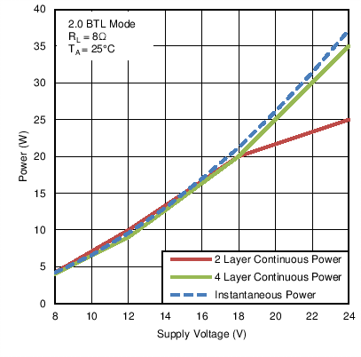
Power vs Supply Voltage (2.0 BTL Mode)

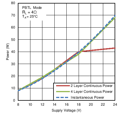
Power vs Supply Voltage (PBTL Mode)
