SCPS222C May 2010 – October 2015 TCA8418E
PRODUCTION DATA.
- 1 Features
- 2 Applications
- 3 Description
- 4 Revision History
- 5 Pin Configuration and Functions
-
6 Specifications
- 6.1 Absolute Maximum Ratings
- 6.2 ESD Ratings
- 6.3 Recommended Operating Conditions
- 6.4 Thermal Information
- 6.5 Electrical Characteristics
- 6.6 I2C Interface Timing Requirements
- 6.7 Reset Timing Requirements for Standard Mode, Fast Mode, Fast Mode Plus (FM+) I2C Bus
- 6.8 Switching Characteristics for Standard Mode, Fast Mode, Fast Mode Plus (FM+) I2C Bus
- 6.9 Keypad Switching Characteristics for Standard Mode, Fast Mode, Fast Mode Plus (FM+) I2C Bus
- 6.10 Typical Characteristics
- 7 Parameter Measurement Information
-
8 Detailed Description
- 8.1 Overview
- 8.2 Functional Block Diagram
- 8.3 Feature Description
- 8.4 Device Functional Modes
- 8.5 Programming
- 8.6
Register Maps
- 8.6.1 Device Address
- 8.6.2
Control Register and Command Byte
- 8.6.2.1 Configuration Register (Address 0x01)
- 8.6.2.2 Interrupt Status Register, INT_STAT (Address 0x02)
- 8.6.2.3 Key Lock and Event Counter Register, KEY_LCK_EC (Address 0x03)
- 8.6.2.4 Key Event Registers (FIFO), KEY_EVENT_A-J (Address 0x04-0x0D)
- 8.6.2.5 Keypad Lock1 to Lock2 Timer Register, KP_LCK_TIMER (Address 0x0E)
- 8.6.2.6 Unlock1 and Unlock2 Registers, UNLOCK1/2 (Address 0x0F-0x10)
- 8.6.2.7 GPIO Interrupt Status Registers, GPIO_INT_STAT1-3 (Address 0x11-0x13)
- 8.6.2.8 GPIO Data Status Registers, GPIO_DAT_STAT1-3 (Address 0x14-0x16)
- 8.6.2.9 GPIO Data Out Registers, GPIO_DAT_OUT1-3 (Address 0x17-0x19)
- 8.6.2.10 GPIO Interrupt Enable Registers, GPIO_INT_EN1-3 (Address 0x1A-0x1C)
- 8.6.2.11 Keypad or GPIO Selection Registers, KP_GPIO1-3 (Address 0x1D-0x1F)
- 8.6.2.12 GPI Event Mode Registers, GPI_EM1-3 (Address 0x20-0x22)
- 8.6.2.13 GPIO Data Direction Registers, GPIO_DIR1-3 (Address 0x23-0x25)
- 8.6.2.14 GPIO Edge/Level Detect Registers, GPIO_INT_LVL1-3 (Address 0x26-0x28)
- 8.6.2.15 Debounce Disable Registers, DEBOUNCE_DIS1-3 (Address 0x29-0x2B)
- 8.6.2.16 GPIO Pullup Disable Register, GPIO_PULL1-3 (Address 0x2C-0x2E)
- 9 Application and Implementation
- 10Power Supply Recommendations
- 11Layout
- 12Device and Documentation Support
- 13Mechanical, Packaging, and Orderable Information
Package Options
Mechanical Data (Package|Pins)
- YFP|25
Thermal pad, mechanical data (Package|Pins)
Orderable Information
9 Application and Implementation
NOTE
Information in the following applications sections is not part of the TI component specification, and TI does not warrant its accuracy or completeness. TI’s customers are responsible for determining suitability of components for their purposes. Customers should validate and test their design implementation to confirm system functionality.
9.1 Application Information
9.1.1 Ghosting Considerations
The TCA8418E supports multiple key presses accurately. Applications requiring three-key combinations (such as <Ctrl><Alt><Del>, or any other combinations) must ensure that the three keys are wired in appropriate key positions to avoid ghosting (or appearing like a 4th key has been pressed).
To avoid ghosting, it is best to keep 3-button combinations that will be pressed on separate rows and columns. Consider the situation with the keypad described in Figure 28
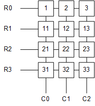 Figure 28. Example Keypad
In the keypad setup in Figure 28, there is a 4x3 keypad matrix, connected to ROW0-ROW3, and COL0-COL2. All of the ROWs are configured as inputs with pullup resistors. The COLs are configured as outputs, driving low. When a key press is made, one of the ROW inputs will be pulled low, letting the TCA8418E know that a key has been pressed, and the TCA8418E will then start the key scanning algorithm. During this algorithm, It will sweep the output low across the columns, such that only 1 column is driven low at a time. While this is done to each column, the TCA8418E will read the ROW inputs, to determine which keys on a column are being pressed.
Ghosting can occur when multiple keys are pressed that can make it appear that additional keys (which are not being pressed) are being pressed.
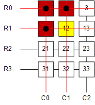 Figure 29. Incorrect 3 Button Combination
In Figure 29, keys 1, 2, and 11 are pressed, which causes a ghosting issue. Since R1 becomes pulled to ground through key 1 (which is pulled through key 2 when C1 is transmitting a low), when C1 is driving low, the TCA8418E will see a low signal at both R0 and R1. This will falsely trigger key 12 as being pressed (the key highlighted as yellow).
The reason for this is that keypad matrices will short the columns to the rows connected together. When C1 is driving low, the low gets transmitted onto R0 via key 2. Key 1 is being pressed, which also shorts C0 to ground. Key 11 is pressed, which then shorts R1 to C0. In this process, R1 is shorted to C1, which is the reason ghosting occurs.
Keypad matrices can support multiple key presses properly, if care is taken when choosing the layout. In Figure 30, we see a 3 button combination which will work as expected. Keys 1, 11, and 21 are pressed (this also is the combination that will set the <Ctrl><Alt><Del> interrupt, see Control-Alt-Delete Support for more information).
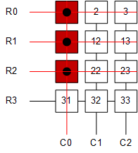 Figure 30. Correct 3 Button Combination
9.2 Typical Application
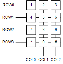
Figure 31 shows a typical application of the TCA8418E. In this specific example, a common 12 key number pad layout is used. This number pad has keys for numbers 0 to 9, *, and #.
9.2.1 Design Requirements
The system designer needs to know a few key pieces in order to design their system for the TCA8418E.
- The number of keys desired
- Whether the keys will be multiplexed or not
- The layout of the multiplexed keys
- Unused keys be tied to VCC through a pullup resistor (10 kΩ)
9.2.2 Detailed Design Procedure
9.2.2.1 Designing the Hardware Layout
The first steps towards designing a keypad array is to determine the desired layout, and to map each key to the appropriate value which will show up in the FIFO. For this example, the number pad below is the physical location of the keys that are desired. The layout is a 4 x 3 array, using rows 0-3 and columns 0-2. For this example, we will not assume any of the other pins will be used.
The following behavior is desired for this example design
- All keys in the keypad array to be added to the FIFO upon a key press
- Attempting to clear the interrupt before the proper registers have been cleared to de-assert the INT pin for 50 μs, then assert the INT pin.
- No additional pins are being used, other than the keypad array
- Keypad lock support, requiring that the unlock combination be ‘#, 1’ which must be pressed within 2 seconds of each other
- Keypad lock interrupt mask timer of 10 seconds to match the back light auto-turn off with 10 seconds of no interrupt
- Hardware debouncing to be enabled
 Figure 32. Example Keypad
Since the TCA8418E will report keys pressed according to the values in the key value table, it will be important to know what the TCA8418E’s values for these key locations are.
According to the key event table, the key presses are assigned in the following way:
Table 26. Key Event Table
| Keypad Button | 1 | 2 | 3 | 4 | 5 | 6 | 7 | 8 | 9 | * | 0 | # |
| Key Event Table Value (Decimal) | 1 | 2 | 3 | 11 | 12 | 13 | 21 | 22 | 23 | 31 | 32 | 33 |
The schematic for this keypad layout is shown in Figure 33, with the key event table values. Note that no external pullup resistors are needed, because the TCA8418E has integrated pullup resistors.
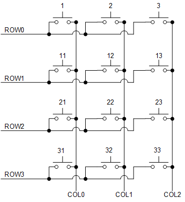 Figure 33. Keypad Schematic
9.2.2.2 Configuring the Registers
The next step to design a keypad array for the TCA8418E is to configure the appropriate hardware registers.
The registers that will need to be modified for the desired features are the following:
Table 27. Registers to Modify
| STEP | REGISTER TO EDIT | VALUE TO WRITE | DESCRIPTION |
|---|---|---|---|
| Setup keypad array | KP_GPIO1 (0x1D) | 0x0F | Set ROW0-ROW3 to KP Matrix |
| KP_GPIO2 (0x1E) | 0x07 | Set COL0-COL2 to KP Matrix | |
| KP_GPIO3 (0x1F) | 0x00 | Set COL8-COL9 to GPIO | |
| Setup Interrupts | CFG (0x01) | 0x95 | Set the KE_IEN, K_LCK_IEN, INT_CFG, and AI bits |
| Setup Unlock Key Combination | UNLOCK1 (0x0F) | 0x21 | Set first unlock key to key 33 |
| UNLOCK2 (0x10) | 0x01 | Set second unlock key to key 1 | |
| Set Keypad Lock Timers | KP_LCK_TIMER (0x0E) | 0x52 | Lock1 to Lock2 set to 2 seconds. Interrupt mask timer set to 10 seconds |
9.2.3 Application Curves
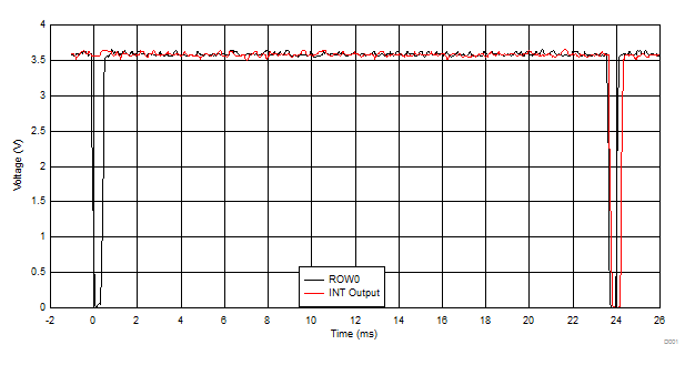 Figure 34. Initial Key Press to Interrupt Output
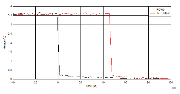 Figure 35. Zoom On Second Scan