SCPS222C May 2010 – October 2015 TCA8418E
PRODUCTION DATA.
- 1 Features
- 2 Applications
- 3 Description
- 4 Revision History
- 5 Pin Configuration and Functions
-
6 Specifications
- 6.1 Absolute Maximum Ratings
- 6.2 ESD Ratings
- 6.3 Recommended Operating Conditions
- 6.4 Thermal Information
- 6.5 Electrical Characteristics
- 6.6 I2C Interface Timing Requirements
- 6.7 Reset Timing Requirements for Standard Mode, Fast Mode, Fast Mode Plus (FM+) I2C Bus
- 6.8 Switching Characteristics for Standard Mode, Fast Mode, Fast Mode Plus (FM+) I2C Bus
- 6.9 Keypad Switching Characteristics for Standard Mode, Fast Mode, Fast Mode Plus (FM+) I2C Bus
- 6.10 Typical Characteristics
- 7 Parameter Measurement Information
-
8 Detailed Description
- 8.1 Overview
- 8.2 Functional Block Diagram
- 8.3 Feature Description
- 8.4 Device Functional Modes
- 8.5 Programming
- 8.6
Register Maps
- 8.6.1 Device Address
- 8.6.2
Control Register and Command Byte
- 8.6.2.1 Configuration Register (Address 0x01)
- 8.6.2.2 Interrupt Status Register, INT_STAT (Address 0x02)
- 8.6.2.3 Key Lock and Event Counter Register, KEY_LCK_EC (Address 0x03)
- 8.6.2.4 Key Event Registers (FIFO), KEY_EVENT_A-J (Address 0x04-0x0D)
- 8.6.2.5 Keypad Lock1 to Lock2 Timer Register, KP_LCK_TIMER (Address 0x0E)
- 8.6.2.6 Unlock1 and Unlock2 Registers, UNLOCK1/2 (Address 0x0F-0x10)
- 8.6.2.7 GPIO Interrupt Status Registers, GPIO_INT_STAT1-3 (Address 0x11-0x13)
- 8.6.2.8 GPIO Data Status Registers, GPIO_DAT_STAT1-3 (Address 0x14-0x16)
- 8.6.2.9 GPIO Data Out Registers, GPIO_DAT_OUT1-3 (Address 0x17-0x19)
- 8.6.2.10 GPIO Interrupt Enable Registers, GPIO_INT_EN1-3 (Address 0x1A-0x1C)
- 8.6.2.11 Keypad or GPIO Selection Registers, KP_GPIO1-3 (Address 0x1D-0x1F)
- 8.6.2.12 GPI Event Mode Registers, GPI_EM1-3 (Address 0x20-0x22)
- 8.6.2.13 GPIO Data Direction Registers, GPIO_DIR1-3 (Address 0x23-0x25)
- 8.6.2.14 GPIO Edge/Level Detect Registers, GPIO_INT_LVL1-3 (Address 0x26-0x28)
- 8.6.2.15 Debounce Disable Registers, DEBOUNCE_DIS1-3 (Address 0x29-0x2B)
- 8.6.2.16 GPIO Pullup Disable Register, GPIO_PULL1-3 (Address 0x2C-0x2E)
- 9 Application and Implementation
- 10Power Supply Recommendations
- 11Layout
- 12Device and Documentation Support
- 13Mechanical, Packaging, and Orderable Information
Package Options
Mechanical Data (Package|Pins)
- YFP|25
Thermal pad, mechanical data (Package|Pins)
Orderable Information
11 Layout
11.1 Layout Guidelines
For printed circuit board (PCB) layout of the TCA8418E, common PCB layout practices should be followed, but additional concerns related to high-speed data transfer, such as matched impedances and differential pairs are not a concern for I2C signal speeds.
In all PCB layouts, it is best practice to avoid right angles in signal traces, to fan out signal traces away from each other upon leaving the vicinity of an integrated circuit (IC), and to use thicker trace widths to carry higher amounts of current that commonly pass through power and ground traces. Bypass and de-coupling capacitors are commonly used to control the voltage on the VCC pin, using a larger capacitor to provide additional power in the event of a short power supply glitch and a smaller capacitor to filter out high-frequency ripple. These capacitors should be placed as close to the TCA8418E as possible.
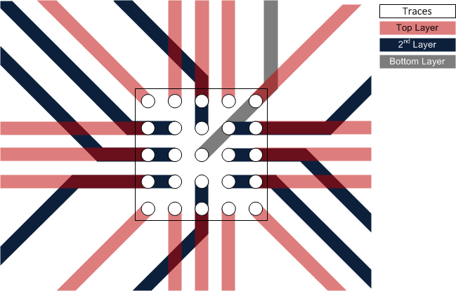
For the layout example provided in Layout Example, a 4 layer board is required to route all of the signals. The layout example shows a way to route the signals out from the device, which can eventually be brought up to the top layer (or any required layer) with the use of a via. This technique is not demonstrated in this example due to the complexity of the layout.
11.2 Layout Example
 Figure 40. YFP Package Layout Example