SBOS766B February 2016 – February 2016 THS3217
PRODUCTION DATA.
- 1 Features
- 2 Applications
- 3 Description
- 4 Revision History
- 5 Device Comparison Table
- 6 Pin Configuration and Functions
-
7 Specifications
- 7.1 Absolute Maximum Ratings
- 7.2 ESD Ratings
- 7.3 Recommended Operating Conditions
- 7.4 Thermal Information
- 7.5 Electrical Characteristics: D2S
- 7.6 Electrical Characteristics: OPS
- 7.7 Electrical Characteristics: D2S + OPS
- 7.8 Electrical Characteristics: Midscale (DC) Reference Buffer
- 7.9 Typical Characteristics: D2S + OPS
- 7.10 Typical Characteristics: D2S Only
- 7.11 Typical Characteristics: OPS only
- 7.12 Typical Characteristics: Midscale (DC) Reference Buffer
- 7.13 Typical Characteristics: Switching Performance
- 7.14 Typical Characteristics: Miscellaneous Performance
- 8 Parameter Measurement Information
-
9 Detailed Description
- 9.1 Overview
- 9.2 Functional Block Diagram
- 9.3 Feature Description
- 9.4 Device Functional Modes
-
10Application and Implementation
- 10.1
Application Information
- 10.1.1
Typical Applications
- 10.1.1.1 High-Frequency, High-Voltage, Dual-Output Line Driver for AWGs
- 10.1.1.2 High-Voltage Pulse-Generator
- 10.1.1.3 Single-Supply, AC-Coupled, Piezo Element Driver
- 10.1.1.4 Output Common-Mode Control Using the Midscale Buffer as a Level Shifter
- 10.1.1.5 Differential I/O Driver With independent Common-Mode Control
- 10.1.1
Typical Applications
- 10.1
Application Information
- 11Power Supply Recommendations
- 12Layout
- 13Device and Documentation Support
- 14Mechanical, Packaging, and Orderable Information
Package Options
Mechanical Data (Package|Pins)
- RGV|16
Thermal pad, mechanical data (Package|Pins)
Orderable Information
12 Layout
12.1 Layout Guidelines
High-speed amplifier designs require careful attention to board layout in order to achieve the performance specified in the data sheets. Poor layout techniques can lead to increased parasitics from the board and external components resulting in suboptimal performance, and also instability in the form of oscillations. The THS3217 evaluation module (EVM) serves as a good reference for proper, high-speed layout methodology. The EVM includes numerous extra elements needed for lab characterization, and also additional features that are useful in certain applications. These additional components can be eliminated on the end system if not required by the application. General suggestions for the design and layout of high-speed, signal-path solutions include:
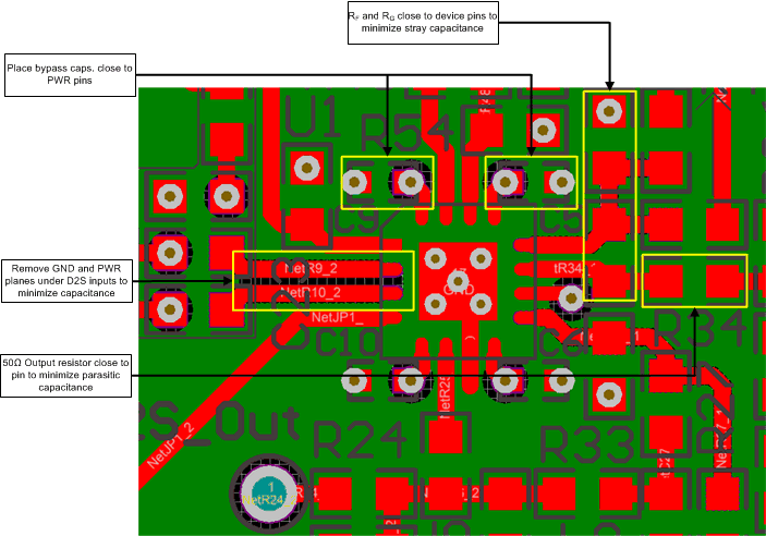
- Minimize parasitic capacitance to any ac ground for all of the signal I/O pins. Parasitic capacitance on the output and input pins can cause instability. To reduce unwanted capacitance, a window around the signal I/O pins should be opened on all of the ground and power planes around those pins. On other areas of the board continuous ground and power planes are preferred for signal routing with matched impedance traces for longer runs.
- Use good, high-frequency decoupling capacitors (0.1 µF) on the ground plane at the device power pins. Higher value capacitors (2.2 µF) are required, but may be placed further from the device power pins and shared among devices. For best high-frequency decoupling, consider X2Y supply-decoupling capacitors that offer a much higher self-resonance frequency over standard capacitors. Avoid narrow power and ground traces to minimize inductance between the pins and the decoupling capacitors. Follow the power-supply guidelines recommended in the Power Supply Recommendations section.
- Careful selection and placement of external components preserve the high-frequency performance of the THS3217. Use low-reactance type resistors. Surface-mount resistors work best, and allow a tighter overall layout. Keep the printed circuit board (PCB) trace length as short as possible. Never use wire-bound type resistors in a high-frequency application. The output pin and inverting input pins are the most sensitive to parasitic capacitance; therefore, always position the feedback and series output resistors, if any, as close as possible to the inverting input pins and output pins. Place other network components, such as input termination resistors, close to the gain-setting resistors.
- When using differential signal routing over any appreciable distance, use microstrip layout techniques with matched impedance traces. On differential lines, like those on the D2S inputs, match the routing in order to minimize common-mode noise effects and improve HD2 performance.
- The input summing junction of the OPS is very sensitive to parasitic capacitance. Connect the RG element into the summing junction with minimal trace length to the device pin side of the resistor. The other side of RG can have more trace length if needed to the source or to ground. For best results, do not socket a high-speed part like the THS3217. The additional lead length and pin-to-pin capacitance introduced by the socket can create an extremely troublesome parasitic network that can make it almost impossible to achieve a smooth, stable frequency response. Best results are obtained by soldering the THS3217 directly onto the board.
12.2 Layout Example
 Figure 107. Layout Example