SLLSEY4A July 2017 – November 2018 THVD1500
PRODUCTION DATA.
- 1 Features
- 2 Applications
- 3 Description
- 4 Revision History
- 5 Pin Configuration and Functions
- 6 Specifications
- 7 Parameter Measurement Information
- 8 Detailed Description
- 9 Application and Implementation
- 10Power Supply Recommendations
- 11Layout
- 12Device and Documentation Support
- 13Mechanical, Packaging, and Orderable Information
Package Options
Refer to the PDF data sheet for device specific package drawings
Mechanical Data (Package|Pins)
- D|8
Thermal pad, mechanical data (Package|Pins)
Orderable Information
7 Parameter Measurement Information
 Figure 8. Measurement of Driver Differential Output Voltage With Common-Mode Load
  Figure 9. Measurement of Driver Differential and Common-Mode Output With RS-485 Load
  Figure 10. Measurement of Driver Differential Output Rise and Fall Times and Propagation Delays
  Figure 11. Measurement of Driver Enable and Disable Times With Active High Output and Pull-Down Load
  Figure 12. Measurement of Driver Enable and Disable Times With Active Low Output and Pull-up Load
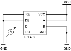
  Figure 13. Measurement of Receiver Output Short Circuit Current
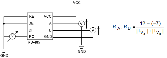
  Figure 14. Measurement of Bus Impedance
  Figure 15. Measurement of Receiver Output Rise and Fall Times and Propagation Delays
  Figure 16. Measurement of Receiver Enable/Disable Times With Driver Enabled
  Figure 17. Measurement of Receiver Enable Times With Driver Disabled