SLVS719G June 2008 – January 2015 TL1963A
PRODUCTION DATA.
- 1 Features
- 2 Applications
- 3 Description
- 4 Revision History
- 5 Description (continued)
- 6 Device Comparison Table
- 7 Pin Configuration and Functions
- 8 Specifications
- 9 Detailed Description
- 10Application and Implementation
- 11Power Supply Recommendations
- 12Layout
- 13Device and Documentation Support
- 14Mechanical, Packaging, and Orderable Information
Package Options
Mechanical Data (Package|Pins)
Thermal pad, mechanical data (Package|Pins)
Orderable Information
1 Features
- Optimized for Fast Transient Response
- Output Current: 1.5 A
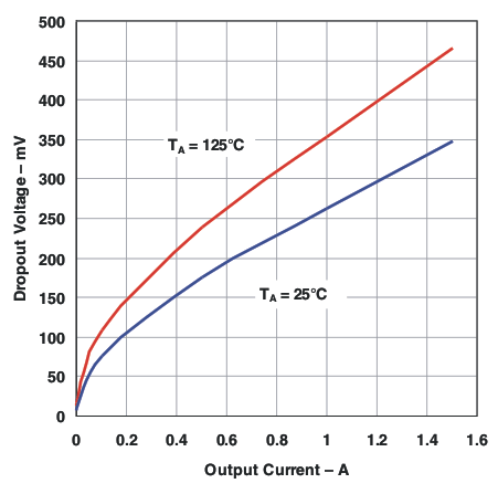
- Dropout Voltage: 340 mV
- Low Noise: 40 μVRMS (10 Hz to 100 kHz)
- 1-mA Quiescent Current
- No Protection Diodes Needed
- Controlled Quiescent Current in Dropout
- Fixed Output Voltages: 1.5 V, 1.8 V, 2.5 V, 3.3 V
- Adjustable Output from 1.21 V to 20 V (TL1963A Only)
- Less Than 1-μA Quiescent Current in Shutdown
- Stable With 10-μF Ceramic Output Capacitor
- Reverse-Battery Protection
- Reverse-Current Protection
2 Applications
- Industrial
- Wireless Infrastructure
- Radio-Frequency Systems
- 3.3-V to 2.5-V Logic Power Supplies
- Post Regulator for Switching Supplies
3 Description
The TL1963A-xx devices are low-dropout (LDO) regulators optimized for fast transient response. The device can supply 1.5 A of output current with a dropout voltage of 340 mV. Operating quiescent current is 1 mA, dropping to less than 1 μA in shutdown. Quiescent current is well controlled; it does not rise in dropout as with many other regulators. In addition to fast transient response, the TL1963A-xx regulators have very low output noise, which makes them ideal for sensitive RF supply applications.
Device Information(1)
| PART NUMBER | PACKAGE | BODY SIZE (NOM) |
|---|---|---|
| TL1963A | SOT (6) | 6.50 mm × 3.50 mm |
| TO-263 (5) | 10.16 mm × 8.42 mm | |
| TL1963A-15 | SOT (6) | 6.50 mm × 3.50 mm |
| SOT (4) | ||
| TO-263 (5) | 10.16 mm × 8.42 mm | |
| TL1963A-18 | SOT (6) | 6.50 mm × 3.50 mm |
| SOT (4) | ||
| TO-263 (5) | 10.16 mm × 8.42 mm | |
| TL1963A-25 | SOT (6) | 6.50 mm × 3.50 mm |
| SOT (4) | ||
| TO-263 (5) | 10.16 mm × 8.42 mm | |
| TL1963A-33 | SOT (6) | 6.50 mm × 3.50 mm |
| SOT (4) | ||
| TO-263 (5) | 10.16 mm × 8.42 mm |
- For all available packages, see the orderable addendum at the end of the data sheet.
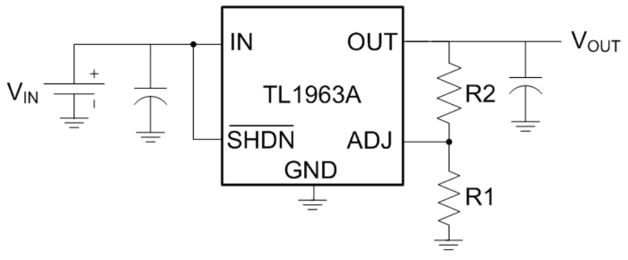
Simplified Schematic
Dropout Voltage vs Output Current