SLVSDQ6A July   2018  – November 2018 TL431LI , TL432LI

PRODUCTION DATA.  

  1. Features
  2. Applications
  3. Description
    1.     Device Images
      1.      Simplified Schematic
  4. Revision History
  5. Device Comparison Table
  6. Pin Configuration and Functions
    1.     Pin Functions
  7. Specifications
    1. 7.1 Absolute Maximum Ratings
    2. 7.2 ESD Ratings
    3. 7.3 Thermal Information
    4. 7.4 Recommended Operating Conditions
    5. 7.5 Electrical Characteristics
    6. 7.6 Typical Characteristics
  8. Parameter Measurement Information
    1. 8.1 Temperature Coefficient
    2. 8.2 Dynamic Impedance
  9. Detailed Description
    1. 9.1 Overview
    2. 9.2 Functional Block Diagram
    3. 9.3 Feature Description
    4. 9.4 Device Functional Modes
      1. 9.4.1 Open Loop (Comparator)
      2. 9.4.2 Closed Loop
  10. 10Applications and Implementation
    1. 10.1 Application Information
    2. 10.2 Typical Applications
      1. 10.2.1 Comparator With Integrated Reference
        1. 10.2.1.1 Design Requirements
        2. 10.2.1.2 Detailed Design Procedure
          1. 10.2.1.2.1 Basic Operation
            1. 10.2.1.2.1.1 Overdrive
          2. 10.2.1.2.2 Output Voltage and Logic Input Level
            1. 10.2.1.2.2.1 Input Resistance
        3. 10.2.1.3 Application Curve
      2. 10.2.2 Precision Constant Current Sink
        1. 10.2.2.1 Design Requirements
        2. 10.2.2.2 Detailed Design Procedure
          1. 10.2.2.2.1 Basic Operation
            1. 10.2.2.2.1.1 Output Current Range and Accuracy
          2. 10.2.2.2.2 Power Consumption
      3. 10.2.3 Shunt Regulator/Reference
        1. 10.2.3.1 Design Requirements
        2. 10.2.3.2 Detailed Design Procedure
          1. 10.2.3.2.1 Programming Output/Cathode Voltage
          2. 10.2.3.2.2 Total Accuracy
          3. 10.2.3.2.3 Stability
          4. 10.2.3.2.4 Start-up Time
        3. 10.2.3.3 Application Curve
      4. 10.2.4 Isolated Flyback with Optocoupler
        1. 10.2.4.1 Design Requirements
          1. 10.2.4.1.1 Detailed Design Procedure
            1. 10.2.4.1.1.1 TL431 Feedback Loop Error Calculation
    3. 10.3 System Examples
  11. 11Power Supply Recommendations
  12. 12Layout
    1. 12.1 Layout Guidelines
    2. 12.2 Layout Example
  13. 13Device and Documentation Support
    1. 13.1 Related Links
    2. 13.2 Documentation Support
      1. 13.2.1 Device Nomenclature
      2. 13.2.2 Related Documentation
    3. 13.3 Receiving Notification of Documentation Updates
    4. 13.4 Community Resources
    5. 13.5 Trademarks
    6. 13.6 Electrostatic Discharge Caution
    7. 13.7 Glossary
  14. 14Mechanical, Packaging, and Orderable Information

Package Options

Mechanical Data (Package|Pins)
Thermal pad, mechanical data (Package|Pins)
Orderable Information

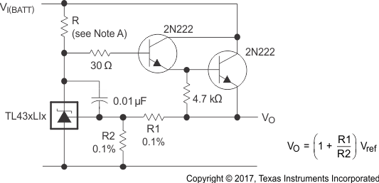
System Examples

TL431LI TL432LI ai_prec_hi_curr_ser_slvsdq6.gif
R should provide cathode current ≥1 mA to the TL431LI at minimum V(BATT).
Figure 27. Precision High-Current Series Regulator
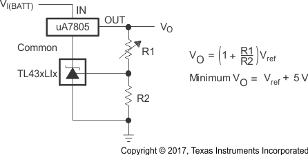
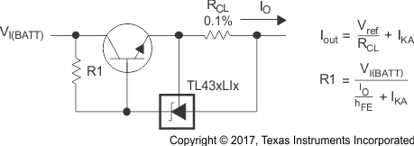
TL431LI TL432LI ai_out_ctrl_3term_slvsdq6.gifFigure 28. Output Control of a Three-Terminal Fixed Regulator
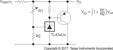
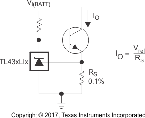
TL431LI TL432LI ai_high_curr_shunt_slvsdq6.gifFigure 29. High-Current Shunt Regulator
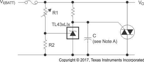
TL431LI TL432LI ai_crowbar_slvsdq6.gif
Refer to the stability boundary conditions in Figure 12 to determine allowable values for C.
Figure 30. Crowbar Circuit
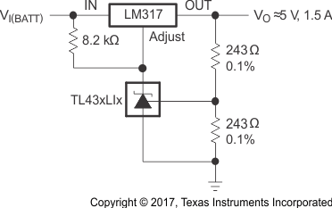
TL431LI TL432LI ai_prec_5v_1p5a_reg_slvsdq6.gifFigure 31. Precision 5-V, 1.5-A Regulator
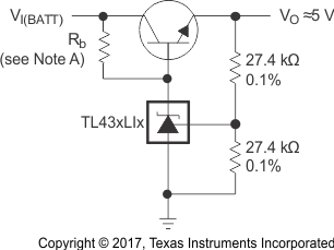
TL431LI TL432LI ai_efficient_5v_slvsdq6.gif
Rb should provide cathode current ≥1 mA to the TL431LI.
Figure 32. Efficient 5-V Precision Regulator
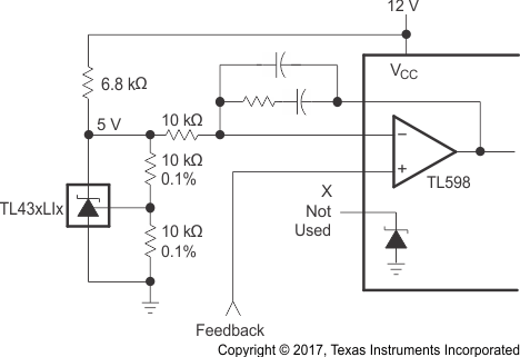
TL431LI TL432LI ai_pwm_conv_slvsdq6.gifFigure 33. PWM Converter With Reference
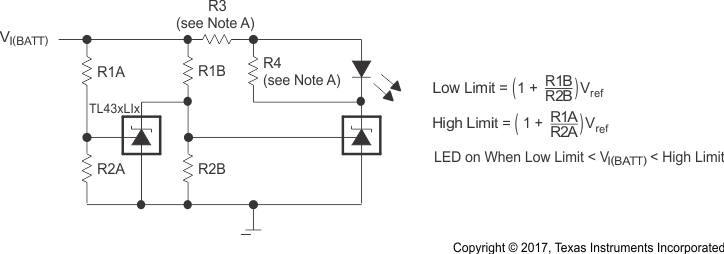
TL431LI TL432LI ai_voltage_monitor_slvsdq6.gif
Select R3 and R4 to provide the desired LED intensity and cathode current ≥1 mA to the TL431LI at the available VI(BATT).
Figure 34. Voltage Monitor
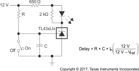
TL431LI TL432LI ai_delay_timer_slvsdq6.gifFigure 35. Delay Timer
TL431LI TL432LI ai_prec_curr_limit_slvsdq6.gifFigure 36. Precision Current Limiter
TL431LI TL432LI ai_prec_const_curr_slvsdq6.gifFigure 37. Precision Constant-Current Sink