SLOS467H October 2006 – January 2015 TL971 , TL972 , TL974
PRODUCTION DATA.
- 1 Features
- 2 Applications
- 3 Description
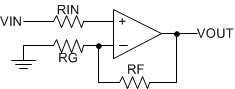
- 4 Simplified Schematic
- 5 Revision History
- 6 Pin Configuration and Functions
- 7 Specifications
- 8 Detailed Description
- 9 Application and Implementation
- 10Power Supply Recommendations
- 11Layout
- 12Device and Documentation Support
- 13Mechanical, Packaging, and Orderable Information
Package Options
Refer to the PDF data sheet for device specific package drawings
Mechanical Data (Package|Pins)
- D|8
- P|8
- DGK|8
- PW|8
Thermal pad, mechanical data (Package|Pins)
Orderable Information
1 Features
- Rail-to-Rail Output Voltage Swing:
±2.4 V at VCC = ±2.5 V - Very Low Noise Level: 4 nV/√Hz
- Ultra-Low Distortion: 0.003%
- High Dynamic Features: 12 MHz, 5 V/μs
- Operating Range: 2.7 V to 12 V
- Latch-Up Performance Exceeds 100 mA Per JESD 78, Class II
- ESD Performance Tested Per JESD 22
- 2000-V Human-Body Model
- 1500-V Charged-Device Model
2 Applications
- Portable Equipment
- Music Players
- Tablets
- Cell Phones
- Instrumentation and Sensors
- Professional Audio Circuits
3 Description
The TL97x family of single, dual, and quad operational amplifiers operates at voltages as low as ±1.35 V and features output rail-to-rail signal swing. The TL97x boast characteristics that make them particularly well suited for portable and battery-supplied equipment. Very low noise and low distortion characteristics make them ideal for audio preamplification.
The TL971 is housed in the space-saving 5-pin SOT-23 package, which simplifies board design because of the ability to be placed anywhere (outside dimensions are 2.8 mm × 2.9 mm).
Device Information(1)
| PART NUMBER | PACKAGE (PIN) | BODY SIZE (NOM) |
|---|---|---|
| TL971 | SOIC (8) | 4.90 mm × 3.90 mm |
| SOT-23 (5) | 2.80 mm × 2.90 mm | |
| TL972 | MSOP (8) | 3.00 mm × 3.00 mm |
| PDIP (8) | 9.60 mm × 6.40 mm | |
| SOIC (8) | 4.90 mm × 3.90 mm | |
| TSSOP (8) | 3.00 mm × 4.40 mm | |
| TL974 | PDIP (14) | 19.30 mm × 6.40 mm |
| SOIC (14) | 8.60 mm × 3.90 mm | |
| TSSOP (14) | 5.00 mm × 4.40 mm |
- For all available packages, see the orderable addendum at the end of the data sheet.
4 Simplified Schematic