SBAS846 November 2017 TLA2021 , TLA2022 , TLA2024
PRODUCTION DATA.
- 1 Features
- 2 Applications
- 3 Description
- 4 Revision History
- 5 Device Comparison Table
- 6 Pin Configuration and Functions
- 7 Specifications
- 8 Detailed Description
- 9 Register Maps
- 10Application and Implementation
- 11Power Supply Recommendations
- 12Layout
- 13Device and Documentation Support
- 14Mechanical, Packaging, and Orderable Information
Package Options
Mechanical Data (Package|Pins)
- RUG|10
Thermal pad, mechanical data (Package|Pins)
Orderable Information
1 Features
- Industry’s Lowest-Cost 12-Bit Delta-Sigma ADCs
- Ultra-Small X2QFN Package: 2 mm × 1.5 mm
- Highly Integrated:
- 4 Single-Ended or 2 Differential Inputs Make the TLA2024 the Industry’s Highest Channel Density ADC (0.75 mm² per Channel)
- PGA (TLA2022 and TLA2024 Only)
- Voltage Reference
- Oscillator
- Low Current Consumption: 150 µA
- Wide Supply Range: 2 V to 5.5 V
- Programmable Data Rate: 128 SPS to 3.3 kSPS
- I2C™ Compatible Interface:
- Supports Standard-Mode and Fast-Mode
- Three Pin-Selectable I2C Addresses
- Operating Temperature Range: –40°C to +85°C
2 Applications
- Personal Electronics:
- TVs, Tablets, Cell Phones
- Wearables
- Drones, Toys
- Home and Kitchen Appliances
- Building Automation:
- HVACs, Smoke Detectors
- Battery Voltage and Current Monitoring
- Temperature Sensing
- Battery-Powered, Portable Instrumentation
3 Description
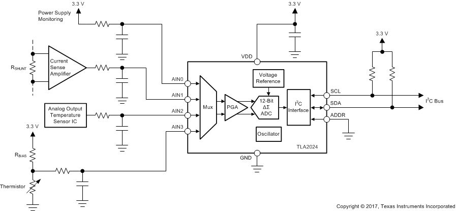
The TLA2021, TLA2022, and TLA2024 devices (TLA202x) are easy-to-use, low-power, 12-bit delta-sigma (ΔΣ) analog-to-digital converters (ADCs) targeted for any type of system-monitoring applications (such as supply or battery voltage supervision, current sensing, or temperature measurements). Offered in an ultra-small, leadless, 10-pin X2QFN package, the TLA2021 and TLA2022 are single-channel ADCs while the TLA2024 features a flexible input multiplexer (MUX) with two differential or four single-ended input measurement options.
The TLA202x integrate a voltage reference and oscillator. Additionally, the TLA2022 and TLA2024 include a programmable gain amplifier (PGA) with selectable input ranges from ±256 mV to ±6.144 V, enabling both large- and small-signal measurements.
The TLA202x communicate via an I2C-compatible interface and operate in either continuous or single-shot conversion mode. The devices automatically power down after one conversion in single-shot conversion mode, significantly reducing power consumption during idle periods.
All of these features, along with a wide operating supply voltage range, make the TLA202x suitable for power- and space-constrained, system-monitoring applications.
Device Information(1)
| PART NUMBER | PACKAGE | BODY SIZE (NOM) |
|---|---|---|
| TLA2021 | X2QFN (10) | 1.50 mm × 2.00 mm |
| TLA2022 | ||
| TLA2024 |
- For all available packages, see the orderable addendum at the end of the data sheet.
System-Monitoring Application Example
