SBAS846 November 2017 TLA2021 , TLA2022 , TLA2024
PRODUCTION DATA.
- 1 Features
- 2 Applications
- 3 Description
- 4 Revision History
- 5 Device Comparison Table
- 6 Pin Configuration and Functions
- 7 Specifications
- 8 Detailed Description
- 9 Register Maps
- 10Application and Implementation
- 11Power Supply Recommendations
- 12Layout
- 13Device and Documentation Support
- 14Mechanical, Packaging, and Orderable Information
Package Options
Mechanical Data (Package|Pins)
- RUG|10
Thermal pad, mechanical data (Package|Pins)
Orderable Information
10 Application and Implementation
NOTE
Information in the following applications sections is not part of the TI component specification, and TI does not warrant its accuracy or completeness. TI’s customers are responsible for determining suitability of components for their purposes. Customers should validate and test their design implementation to confirm system functionality.
10.1 Application Information
The following sections give example circuits and suggestions for using the TLA202x in various applications.
10.1.1 Basic Interface Connections
Figure 18 shows the principle I2C connections for the TLA202x.
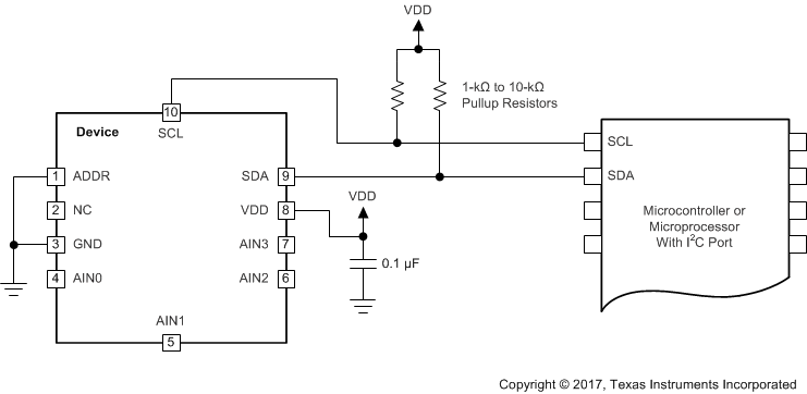 Figure 18. Typical Interface Connections of the TLA202x
The TLA202x interface directly to standard-mode or fast-mode I2C controllers. Any microcontroller I2C peripheral, including master-only and single-master I2C peripherals, operates with the TLA202x. The TLA202x do not perform clock-stretching (that is, the devices never pull the clock line low), so this function does not need to be provided for unless other clock-stretching devices are present on the same I2C bus.
Pullup resistors are required on both the SDA and SCL lines because I2C bus drivers are open-drain. The size of these resistors depends on the bus operating speed and capacitance of the bus lines. Higher-value resistors yield lower power consumption when the bus lines are pulled low, but increase the transition times on the bus, which limits the bus speed. Lower-value resistors allow higher interface speeds, but at the expense of higher power consumption when the bus lines are pulled low. Long bus lines have higher capacitance and require smaller pullup resistors to compensate. Do not use resistors that are too small because the bus drivers may be unable to pull the bus lines low.
See the I2C-Bus Specification and User Manual from NXP Semiconductors for more details on pullup resistor sizing.
10.1.2 Connecting Multiple Devices
Up to three TLA202x devices can be connected to a single I2C bus by using different address pin configurations for each device. Use the address pin to set the TLA202x to one of three different I2C addresses. Figure 19 shows an example with three TLA202x devices on the same I2C bus. One set of pullup resistors is required per bus line. The pullup resistor values may need to decrease to compensate for the additional bus capacitance presented by multiple devices and increased line length.
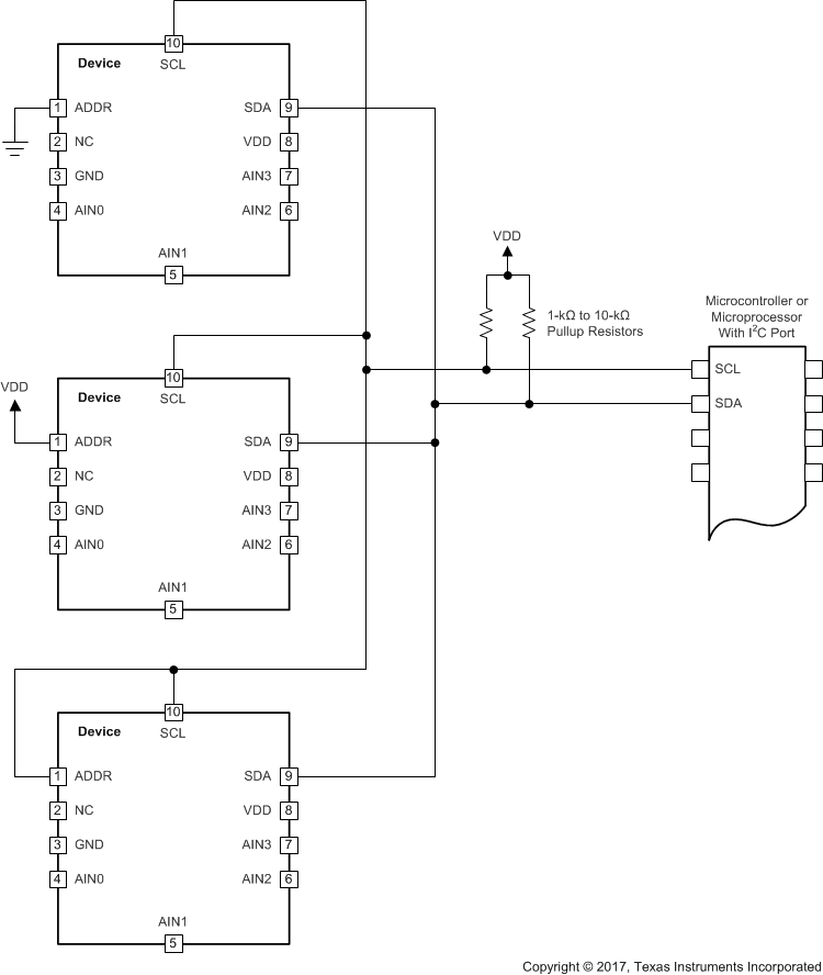
NOTE:
The TLA202x power and input connections are omitted for clarity. The ADDR pin selects the I2C address.10.1.3 Single-Ended Signal Measurements
The TLA2021 and TLA2022 can measure one single-ended signal, and the TLA2024 up to four single-ended signals. To measure single-ended signals with the TLA2021 and TLA2022, connect AIN1 to GND externally. The TLA2024 measures single-ended signals by properly configuring the MUX[2:0] bits (settings 100 to 111) in the configuration register. Figure 20 shows a single-ended connection scheme for the TLA2024 highlighted in red (a differential connection scheme is shown in green). The single-ended signal range is from 0 V up to the positive supply or +FS (whichever is lower). Negative voltages cannot be applied to these devices because the TLA202x can only accept positive voltages with respect to ground. Only the code range from 0000h to 7FF0h (or a subset thereof in case +FS > VDD) is used in this case.
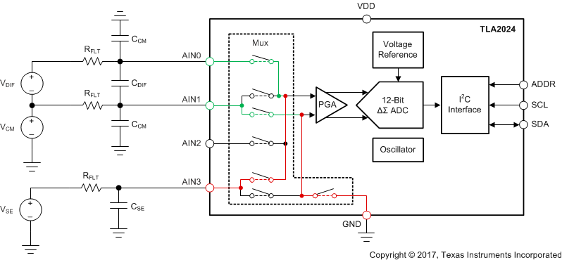 Figure 20. Filter Implementation for Single-Ended and Differential Signal Measurements
The TLA2024 also allows AIN3 to serve as a common point for measurements by appropriately setting the MUX[2:0] bits. AIN0, AIN1, and AIN2 can all be measured with respect to AIN3. In this configuration, the usable voltage and code range, respectively, is increased over the single-ended configuration because negative differential voltages are allowed when GND < V(AIN3) < VDD. Assume the following settings for example: VDD = 5 V, FSR = ±2.048 V, AINP = AIN0, and AINN = AIN3 = 2.5 V. In this case, the voltage at AIN0 can swing from V(AIN0) = 2.5 V – 2.048 V to 2.5 V + 2.048 V using the entire full-scale range.
10.1.4 Analog Input Filtering
Analog input filtering serves two purposes:
- Limits the effect of aliasing during the ADC sampling process
- Attenuates unwanted noise components outside the bandwidth of interest
In most cases, a first-order resistor capacitor (RC) filter is sufficient to completely eliminate aliasing or to reduce the effect of aliasing to a level within the noise floor of the sensor. A good starting point for a system design with the TLA202x is to use a differential RC filter with a cutoff frequency set somewhere between the selected output data rate and 25 kHz. Make the series resistor values as small as possible to reduce voltage drops across the resistors caused by the device input currents to a minimum. However, the resistors should be large enough to limit the current into the analog inputs to less than 10 mA in the event of an overvoltage. Then choose the differential capacitor value to achieve the target filter cutoff frequency. Common-mode filter capacitors to GND can be added as well, but should always be at least ten times smaller than the differential filter capacitor.
Figure 20 shows an example of filtering a differential signal (AIN0, AIN1), and a single-ended signal (AIN3). Equation 3 and Equation 4 show how to calculate the filter cutoff frequencies (fCO) in the differential and single-ended cases, respectively.
10.1.5 Duty Cycling To Reduce Power Consumption
For applications where power consumption is critical, the TLA202x support duty cycling that yield significant power savings by periodically requesting high data rate readings at an effectively lower data rate. For example, an TLA202x in power-down state with a data rate set to 3300 SPS can be operated by a microcontroller that instructs a single-shot conversion every 7.81 ms (128 SPS). A conversion at 3300 SPS requires approximately 0.3 ms, so the TLA202x enters power-down state for the remaining 7.51 ms. In this configuration, the TLA202x consume approximately 1/25th the power that is otherwise consumed in continuous-conversion mode. The duty cycling rate is arbitrary and is defined by the master controller.
10.1.6 I2C Communication Sequence Example
This section provides an example of an I2C communication sequence between a microcontroller (the master) and a TLA2024 (the slave) configured with a slave address of 1001 000 to start a single-shot conversion and subsequently read the conversion result.
- Write the configuration register as shown in Figure 21 to configure the device (for example, write MUX[2:0] = 000, PGA[2:0] = 010, MODE = 1, and DR[2:0] = 110) and start a single-shot conversion (OS = 1):
- Wait at least t = 1 / DR ± 10% for the conversion to complete.
- Then, as shown in Figure 23, read the conversion data register:
- Start a new single-shot conversion by writing a 1 to the OS bit in the configuration register.
 Figure 21. Write the Configuration Register
Alternatively, poll the OS bit for a 1 as shown in Figure 22 to determine when the conversion result is ready for retrieval. This option does not work in continuous-conversion mode because the OS bit always reads 0.
 Figure 22. Read the Configuration Register to Check for OS = 1
 Figure 23. Read the Conversion Data Register
To save time, a new conversion can also be started (step 4) before reading the conversion result (step 3). Figure 24 lists a legend for Figure 21 to Figure 23.
 Figure 24. Legend for the I2C Sequence Diagrams
10.2 Typical Application
This application example describes how to use the TLA2024 to monitor two different supply voltage rails in a system. Figure 25 shows a typical implementation for monitoring two supply voltage rails.
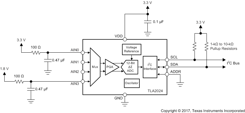 Figure 25. Monitoring Two Supply Voltage Rails Using the TLA2024
10.2.1 Design Requirements
Table 8 lists the design requirements for this application.
Table 8. Design Requirements
| DESIGN PARAMETER | VALUE |
|---|---|
| Device supply voltage | 3.3 V |
| Voltage rails to monitor | 1.8 V, 3.3 V |
| Measurement accuracy | ±0.5% |
| Update rate | 1 ms per rail |
10.2.2 Detailed Design Procedure
The analog inputs, AIN0 and AIN3, connect directly to the supply voltage rails that are monitored through RC filter resistors. Small filter resistor values of 100 Ω are chosen to reduce voltage drops, and therefore offset errors, caused by the input currents of the TLA2024 to a minimum. Filter capacitors of 0.47 µF are chosen to set the filter cutoff frequencies at 3.39 kHz. In order to get one reading from each of the two supplies within 2 ms, a data rate of 2400 SPS is selected. The device is set up for single-ended measurements using MUX[2:0] settings 100 and 101. A FSR = ±4.096 V is selected to measure the 3.3-V rail. The same FSR can also be used to measure the 1.8-V rail or the FSR can be set to FSR = ±2.048 V.
10.2.3 Application Curve
The measurement results in Figure 26 show that the two supplies can be measured with ±0.5% accuracy over the complete operating ambient temperature range without any offset or gain calibration.
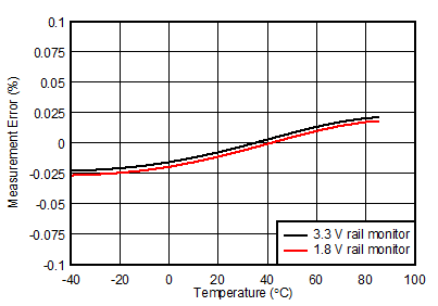 Figure 26. Measurement Error vs Temperature