SBAS846 November 2017 TLA2021 , TLA2022 , TLA2024
PRODUCTION DATA.
- 1 Features
- 2 Applications
- 3 Description
- 4 Revision History
- 5 Device Comparison Table
- 6 Pin Configuration and Functions
- 7 Specifications
- 8 Detailed Description
- 9 Register Maps
- 10Application and Implementation
- 11Power Supply Recommendations
- 12Layout
- 13Device and Documentation Support
- 14Mechanical, Packaging, and Orderable Information
Package Options
Mechanical Data (Package|Pins)
- RUG|10
Thermal pad, mechanical data (Package|Pins)
Orderable Information
8 Detailed Description
8.1 Overview
The TLA202x are a family of very small, low-power, 12-bit, delta-sigma (ΔΣ) analog-to-digital converters (ADCs). The TLA202x consist of a ΔΣ ADC core with an internal voltage reference, a clock oscillator, and an I2C interface. The TLA2022 and TLA2024 also integrate a programmable gain amplifier (PGA). Figure 5, Figure 6, and Figure 7 show the functional block diagrams of the TLA2024, TLA2022, and TLA2021, respectively.
The TLA202x ADC core measures a differential signal, VIN, that is the difference of VAINP and VAINN. The converter core consists of a differential, switched-capacitor ΔΣ modulator followed by a digital filter. This architecture results in a very strong attenuation of any common-mode signals. Input signals are compared to the internal voltage reference. The digital filter receives a high-speed bitstream from the modulator and outputs a code proportional to the input voltage.
The TLA202x have two available conversion modes: single-shot and continuous-conversion. In single-shot conversion mode, the ADC performs one conversion of the input signal upon request, stores the conversion value to an internal conversion register, and then enters a power-down state. This mode is intended to provide significant power savings in systems that only require periodic conversions or when there are long idle periods between conversions. In continuous-conversion mode, the ADC automatically begins a conversion of the input signal as soon as the previous conversion is complete. The rate of continuous conversion is equal to the programmed data rate. Data can be read at any time and always reflect the most recently completed conversion.
8.2 Functional Block Diagrams
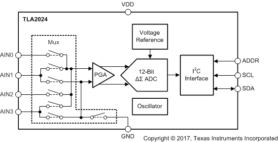 Figure 5. TLA2024 Block Diagram
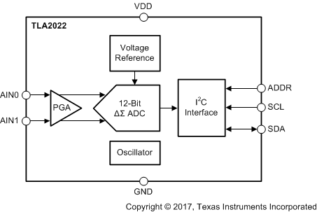 Figure 6. TLA2022 Block Diagram
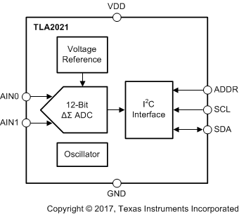 Figure 7. TLA2021 Block Diagram
8.3 Feature Description
8.3.1 Multiplexer
Figure 8 shows that the TLA2024 contains an analog input multiplexer (MUX). Four single-ended or two differential signals can be measured. Additionally, AIN0 and AIN1 can be measured differentially to AIN3. The multiplexer is configured by bits MUX[2:0] in the configuration register. When single-ended signals are measured, the negative input of the ADC is internally connected to GND by a switch within the multiplexer.
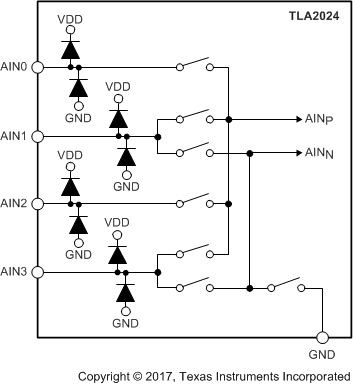 Figure 8. Input Multiplexer
The TLA2021 and TLA2022 do not have an input multiplexer and can either measure one differential signal or one single-ended signal. For single-ended measurements, connect the AIN1 pin to GND externally. In subsequent sections of this data sheet, AINP refers to AIN0 and AINN refers to AIN1 for the TLA2021 and TLA2022.
Electrostatic discharge (ESD) diodes connected to VDD and GND protect the TLA202x analog inputs. Keep the absolute voltage on any input within the range shown in Equation 1 to prevent the ESD diodes from turning on.
If the voltages on the analog input pins can potentially violate these conditions, use external Schottky diodes and series resistors to limit the input current to safe values (see the Absolute Maximum Ratings table).
8.3.2 Analog Inputs
The TLA202x use a switched-capacitor input stage where capacitors are continuously charged and then discharged to measure the voltage between AINP and AINN. The frequency at which the input signal is sampled is referred to as the sampling frequency or the modulator frequency (fMOD). The TLA202x have a 1-MHz internal oscillator that is further divided by a factor of 4 to generate fMOD at 250 kHz. The capacitors used in this input stage are small, and to external circuitry, the average loading appears resistive. Figure 9 shows this structure. The capacitor values set the resistance and switching rate. Figure 10 shows the timing for the switches in Figure 9. During the sampling phase, switches S1 are closed. This event charges CA1 to VAINP, CA2 to VAINN, and CB to (VAINP – VAINN). During the discharge phase, S1 is first opened and then S2 is closed. CA1 and CA2 then discharge to approximately 0.7 V and CB discharges to 0 V. This charging draws a very small transient current from the source driving the TLA202x analog inputs. The average value of this current can be used to calculate the effective impedance (Zeff), where Zeff = VIN / IAVERAGE.
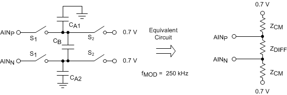 Figure 9. Simplified Analog Input Circuit
 Figure 10. S1 and S2 Switch Timing
The common-mode input impedance is measured by applying a common-mode signal to the shorted AINP and AINN inputs and measuring the average current consumed by each pin. The common-mode input impedance changes depending on the full-scale range, but is approximately 6 MΩ for the default full-scale range. In Figure 9, the common-mode input impedance is ZCM.
The differential input impedance is measured by applying a differential signal to the AINP and AINN inputs where one input is held at 0.7 V. The current that flows through the pin connected to 0.7 V is the differential current and scales with the full-scale range. In Figure 9, the differential input impedance is ZDIFF.
Consider the typical value of the input impedance. Unless the input source has a low impedance, the TLA202x input impedance may affect the measurement accuracy. For sources with high-output impedance, buffering may be necessary. Active buffers introduce noise, offset, and gain errors. Consider all of these factors in high-accuracy applications.
The clock oscillator frequency drifts slightly with temperature; therefore, the input impedances also drift. For most applications, this input impedance drift is negligible and can be ignored.
8.3.3 Full-Scale Range (FSR) and LSB Size
A programmable gain amplifier (PGA) is implemented before the ΔΣ ADC of the TLA2022 and TLA2024. The full-scale range is configured by bits PGA[2:0] in the configuration register and can be set to ±6.144 V, ±4.096 V, ±2.048 V, ±1.024 V, ±0.512 V, or ±0.256 V. Table 1 shows the FSR together with the corresponding LSB size. Equation 2 shows how to calculate the LSB size from the selected full-scale range.
Table 1. Full-Scale Range and Corresponding LSB Size
| FSR | LSB SIZE |
|---|---|
| ±6.144 V(1) | 3 mV |
| ±4.096 V(1) | 2 mV |
| ±2.048 V | 1 mV |
| ±1.024 V | 0.5 mV |
| ±0.512 V | 0.25 mV |
| ±0.256 V | 0.125 mV |
The FSR of the TLA2021 is fixed at ±2.048 V.
Analog input voltages must never exceed the analog input voltage limits given in the Absolute Maximum Ratings table. If a VDD supply voltage greater than 4 V is used, the ±6.144-V full-scale range allows input voltages to extend up to the supply. Although in this case (or whenever the supply voltage is less than the full-scale range) a full-scale ADC output code cannot be obtained. For example, with VDD = 3.3 V and FSR = ±4.096 V, only signals up to VIN = ±3.3 V can be measured. The code range that represents voltages |VIN| > 3.3 V is not used in this case.
8.3.4 Voltage Reference
The TLA202x have an integrated voltage reference. An external reference cannot be used with these devices. Errors associated with the initial voltage reference accuracy and the reference drift with temperature are included in the gain error and gain drift specifications in the Electrical Characteristics table.
8.3.5 Oscillator
The TLA202x have an integrated oscillator running at 1 MHz. No external clock can be applied to operate these devices. The internal oscillator drifts over temperature and time. The output data rate scales proportionally with the oscillator frequency.
8.3.6 Output Data Rate and Conversion Time
The TLA202x offer programmable output data rates. Use the DR[2:0] bits in the configuration register to select output data rates of 128 SPS, 250 SPS, 490 SPS, 920 SPS, 1600 SPS, 2400 SPS, or 3300 SPS.
Conversions in the TLA202x settle within a single cycle, which means the conversion time equals 1 / DR.
8.4 Device Functional Modes
8.4.1 Reset and Power-Up
The TLA202x reset on power-up and set all bits in the configuration register to the respective default settings. The TLA202x enter a power-down state after completion of the reset process. The device interface and digital blocks are active, but no data conversions are performed. The initial power-down state of the TLA202x relieves systems with tight power-supply requirements from encountering a surge during power-up.
The TLA202x respond to the I2C general-call reset command. When the TLA202x receive a general-call reset command (06h), an internal reset is performed as if the device is powered up.
8.4.2 Operating Modes
The TLA202x operate in one of two modes: continuous-conversion or single-shot. The MODE bit in the configuration register selects the respective operating mode.
8.4.2.1 Single-Shot Conversion Mode
When the MODE bit in the configuration register is set to 1, the TLA202x enter a power-down state, and operate in single-shot conversion mode. This power-down state is the default state for the TLA202x when power is first applied. Although powered down, the devices respond to commands. The TLA202x remain in this power-down state until a 1 is written to the operational status (OS) bit in the configuration register. When the OS bit is asserted, the device powers up in approximately 25 µs, resets the OS bit to 0, and starts a single conversion. When conversion data are ready for retrieval, the OS bit is set to 1 and the device powers down again. Writing a 1 to the OS bit while a conversion is ongoing has no effect. To switch to continuous-conversion mode, write a 0 to the MODE bit in the configuration register.
8.4.2.2 Continuous-Conversion Mode
In continuous-conversion mode (MODE bit set to 0), the TLA202x perform conversions continuously. When a conversion is complete, the TLA202x place the result in the conversion data register and immediately begin another conversion. When writing new configuration settings, the currently ongoing conversion completes with the previous configuration settings. Thereafter, continuous conversions with the new configuration settings start. To switch to single-shot conversion mode, write a 1 to the MODE bit in the configuration register or reset the device.
8.5 Programming
8.5.1 I2C Interface
The TLA202x use an I2C-compatible (inter-integrated circuit) interface for serial communication. I2C is a 2-wire, open-drain communication interface that allows communication of a master device with multiple slave devices on the same bus through the use of device addressing. Each slave device on an I2C bus must have a unique address. Communication on the I2C bus always takes place between two devices: one acting as the master and the other as the slave. Both the master and slave can receive and transmit data, but the slave can only read or write under the direction of the master. The TLA202x always act as I2C slave devices.
An I2C bus consists of two lines: SDA and SCL. SDA carries data and SCL provides the clock. Devices on the I2C bus drive the bus lines low by connecting the lines to ground; the devices never drive the bus lines high. Instead, the bus wires are pulled high by pullup resistors; thus, the bus wires are always high when a device is not driving the lines low. As a result of this configuration, two devices do not conflict. If two devices drive the bus simultaneously, there is no driver contention.
See the I2C-Bus Specification and User Manual from NXP Semiconductors™ for more details.
8.5.1.1 I2C Address Selection
The TLA202x have one address pin (ADDR) that configures the I2C address of the device. The ADDR pin can connect to GND, VDD, or SCL (as shown in Table 2), which allows three different addresses to be selected with one pin. At the start of every transaction, that is between the START condition (first falling edge of SDA) and the first falling SCL edge of the address byte, the TLA202x decode its address configuration again.
Table 2. ADDR Pin Connection and Corresponding Slave Address
| ADDR PIN CONNECTION | SLAVE ADDRESS |
|---|---|
| GND | 1001 000 |
| VDD | 1001 001 |
| SCL | 1001 011 |
8.5.1.2 I2C Interface Speed
The TLA202x support I2C interface speeds up to 400 kbit/s. Standard-mode (Sm) with bit rates up to 100 kbit/s, and fast-mode (Fm) with bit rates up to 400 kbit/s are supported. Fast-mode plus (Fm+) and high-speed mode (Hs-mode) are not supported.
8.5.1.3 Serial Clock (SCL) and Serial Data (SDA)
The serial clock (SCL) line is used to clock data in and out of the device. The master always drives the clock line. The TLA202x cannot act as a master and as a result can never drive SCL.
The serial data (SDA) line allows for bidirectional communication between the host (the master) and the TLA202x (the slave). When the master reads from a TLA202x, the TLA202x drives the data line; when the master writes to a TLA202x, the master drives the data line.
Data on the SDA line must be stable during the high period of the clock. The high or low state of the data line can only change when the SCL line is low. One clock pulse is generated for each data bit transferred. When in an idle state, the master should hold SCL high.
8.5.1.4 I2C Data Transfer Protocol
Figure 11 shows the format of the data transfer. The master initiates all transactions with the TLA202x by generating a START (S) condition. A high-to-low transition on the SDA line while SCL is high defines a START condition. The bus is considered to be busy after the START condition.
Following the START condition, the master sends the 7-bit slave address corresponding to the address of the TLA202x that the master wants to communicate with. The master then sends an eighth bit that is a data direction bit (R/W). An R/W bit of 0 indicates a write operation, and an R/W bit of 1 indicates a read operation. After the R/W bit, the master generates a ninth SCLK pulse and releases the SDA line to allow the TLA202x to acknowledge (ACK) the reception of the slave address by pulling SDA low. In case the device does not recognize the slave address, the TLA202x holds SDA high to indicate a not acknowledge (NACK) signal.
Next follows the data transmission. If the transaction is a read (R/W = 1), the TLA202x outputs data on SDA. If the transaction is a write (R/W = 0), the host outputs data on SDA. Data are transferred byte-wise, most significant bit (MSB) first. The number of bytes that can be transmitted per transfer is unrestricted. Each byte must be acknowledged (via the ACK bit) by the receiver. If the transaction is a read, the master issues the ACK. If the transaction is a write, the TLA202x issues the ACK.
The master terminates all transactions by generating a STOP (P) condition. A low-to-high transition on the SDA line while SCL is high defines a STOP condition. The bus is considered free again tBUF (bus-free time) after the STOP condition.
 Figure 11. I2C Data Transfer Format
8.5.1.5 Timeout
The TLA202x offer a I2C timeout feature that can be used to recover communication when a serial interface transmission is interrupted. If the host initiates contact with the TLA202x but subsequently remains idle for 25 ms before completing a command, the TLA202x interface is reset. If the TLA202x interface resets because of a timeout condition, the host must abort the transaction and restart the communication again by issuing a new START condition.
8.5.1.6 I2C General-Call (Software Reset)
The TLA202x respond to the I2C general-call address (0000 000) if the R/W bit is 0. The devices acknowledge the general-call address and, if the next byte is 06h, the TLA202x reset the internal registers and enter a power-down state.
8.5.2 Reading and Writing Register Data
The host can read the conversion data register from the TLA202x, or read and write the configuration register from and to the TLA202x, respectively. The value of the register pointer (RP), which is the first data byte after the slave address of a write transaction (R/W = 0), determines the register that is addressed. Table 3 shows the mapping between the register pointer value and the register that is addressed.
Register data are sent with the most significant byte first, followed by the least significant byte. Within each byte, data are transmitted most significant bit first.
Table 3. Register Pointer (RP)
| REGISTER POINTER (Hex) | REGISTER |
|---|---|
| 00h | Conversion data register |
| 01h | Configuration register |
8.5.2.1 Reading Conversion Data or the Configuration Register
Read the conversion data register or configuration register as shown in Figure 12 by using two I2C communication frames. The first frame is an I2C write operation where the R/W bit at the end of the slave address is 0 to indicate a write. In this frame, the host sends the register pointer that points to the register to read from. The second frame is an I2C read operation where the R/W bit at the end of the slave address is 1 to indicate a read. The TLA202x transmits the contents of the register in this second I2C frame. The master can terminate the transmission after any byte by not acknowledging or issuing a START or STOP condition.
When repeatedly reading the same register, the register pointer does not need to be written every time again because the TLA202x store the value of the register pointer until a write operation modifies the value.

8.5.2.2 Writing the Configuration Register
Write the configuration register as shown in Figure 13 using a single I2C communication frame. The R/W bit at the end of the salve address is 0 to indicate a write. The host first sends the register pointer that points to the configuration register, followed by two bytes that represent the register content to write. The TLA202x acknowledge each received byte.
 Figure 13. Writing Register Data
Figure 14 provides a legend for Figure 12 and Figure 13.
 Figure 14. Legend for the I2C Sequence Diagrams
8.5.3 Data Format
The TLA202x provide 12 bits of data in binary two's-complement format that is left-justified within the 16-bit data word. A positive full-scale (+FS) input produces an output code of 7FF0h and a negative full-scale (–FS) input produces an output code of 8000h. The output clips at these codes for signals that exceed full-scale. Table 4 summarizes the ideal output codes for different input signals. Figure 15 shows code transitions versus input voltage.
Table 4. Input Signal Versus Ideal Output Code
| INPUT SIGNAL VIN = (VAINP – VAINN) |
IDEAL OUTPUT CODE(1) |
|---|---|
| ≥ +FS (211 – 1) / 211 | 7FF0h |
| +FS / 211 | 0010h |
| 0 | 0000h |
| –FS / 211 | FFF0h |
| ≤ –FS | 8000h |
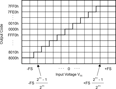 Figure 15. Code Transition Diagram
NOTE
Single-ended signal measurements, where VAINN = 0 V and VAINP = 0 V to +FS, only use the positive code range from 0000h to 7FF0h. However, because of device offset, the TLA202x can still output negative codes in case VAINP is close to 0 V.