SBAS846 November   2017 TLA2021 , TLA2022 , TLA2024

PRODUCTION DATA.  

  1. Features
  2. Applications
  3. Description
  4. Revision History
  5. Device Comparison Table
  6. Pin Configuration and Functions
  7. Specifications
    1. 7.1 Absolute Maximum Ratings
    2. 7.2 ESD Ratings
    3. 7.3 Recommended Operating Conditions
    4. 7.4 Thermal Information
    5. 7.5 Electrical Characteristics
    6. 7.6 I2C Timing Requirements
    7. 7.7 Typical Characteristics
  8. Detailed Description
    1. 8.1 Overview
    2. 8.2 Functional Block Diagrams
    3. 8.3 Feature Description
      1. 8.3.1 Multiplexer
      2. 8.3.2 Analog Inputs
      3. 8.3.3 Full-Scale Range (FSR) and LSB Size
      4. 8.3.4 Voltage Reference
      5. 8.3.5 Oscillator
      6. 8.3.6 Output Data Rate and Conversion Time
    4. 8.4 Device Functional Modes
      1. 8.4.1 Reset and Power-Up
      2. 8.4.2 Operating Modes
        1. 8.4.2.1 Single-Shot Conversion Mode
        2. 8.4.2.2 Continuous-Conversion Mode
    5. 8.5 Programming
      1. 8.5.1 I2C Interface
        1. 8.5.1.1 I2C Address Selection
        2. 8.5.1.2 I2C Interface Speed
        3. 8.5.1.3 Serial Clock (SCL) and Serial Data (SDA)
        4. 8.5.1.4 I2C Data Transfer Protocol
        5. 8.5.1.5 Timeout
        6. 8.5.1.6 I2C General-Call (Software Reset)
      2. 8.5.2 Reading and Writing Register Data
        1. 8.5.2.1 Reading Conversion Data or the Configuration Register
        2. 8.5.2.2 Writing the Configuration Register
      3. 8.5.3 Data Format
  9. Register Maps
    1. 9.1 Conversion Data Register (RP = 00h) [reset = 0000h]
    2. 9.2 Configuration Register (RP = 01h) [reset = 8583h]
  10. 10Application and Implementation
    1. 10.1 Application Information
      1. 10.1.1 Basic Interface Connections
      2. 10.1.2 Connecting Multiple Devices
      3. 10.1.3 Single-Ended Signal Measurements
      4. 10.1.4 Analog Input Filtering
      5. 10.1.5 Duty Cycling To Reduce Power Consumption
      6. 10.1.6 I2C Communication Sequence Example
    2. 10.2 Typical Application
      1. 10.2.1 Design Requirements
      2. 10.2.2 Detailed Design Procedure
      3. 10.2.3 Application Curve
  11. 11Power Supply Recommendations
    1. 11.1 Power-Supply Sequencing
    2. 11.2 Power-Supply Decoupling
  12. 12Layout
    1. 12.1 Layout Guidelines
    2. 12.2 Layout Example
  13. 13Device and Documentation Support
    1. 13.1 Device Support
      1. 13.1.1 Third-Party Products Disclaimer
    2. 13.2 Related Links
    3. 13.3 Receiving Notification of Documentation Updates
    4. 13.4 Community Resources
    5. 13.5 Trademarks
    6. 13.6 Electrostatic Discharge Caution
    7. 13.7 Glossary
  14. 14Mechanical, Packaging, and Orderable Information

Package Options

Mechanical Data (Package|Pins)
Thermal pad, mechanical data (Package|Pins)
Orderable Information

Power Supply Recommendations

The device requires a single unipolar supply (VDD) to power the analog and digital circuitry of the device.

Power-Supply Sequencing

Wait approximately 50 µs after VDD is stabilized before communicating with the device to allow the power-up reset process to complete.

Power-Supply Decoupling

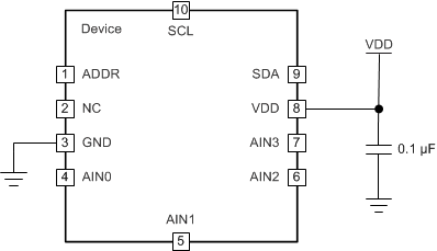
Good power-supply decoupling is important to achieve optimum performance. As shown in Figure 27, VDD must be decoupled with at least a 0.1-µF capacitor to GND. The 0.1-µF bypass capacitor supplies the momentary bursts of extra current required from the supply when the device is converting. Place the bypass capacitor as close to the power-supply pin of the device as possible using low-impedance connections. Use multilayer ceramic chip capacitors (MLCCs) that offer low equivalent series resistance (ESR) and inductance (ESL) characteristics for power-supply decoupling purposes. For very sensitive systems, or for systems in harsh noise environments, avoid using vias to connect the capacitors to the device pins for better noise immunity. The use of multiple vias in parallel lowers the overall inductance and is beneficial for connections to ground planes.
TLA2021 TLA2022 TLA2024 ai_supply_decoupling_bas822.gif Figure 27. TLA202x Power-Supply Decoupling