SLVS695D June 2007 – January 2015 TLC5916 , TLC5917
PRODUCTION DATA.
- 1 Features
- 2 Applications
- 3 Description
- 4 Revision History
- 5 Device Comparison Table
- 6 Pin Configuration and Functions
-
7 Specifications
- 7.1 Absolute Maximum Ratings
- 7.2 ESD Ratings
- 7.3 Recommended Operating Conditions
- 7.4 Thermal Information
- 7.5 Electrical Characteristics: VDD = 3 V
- 7.6 Electrical Characteristics: VDD = 5.5 V
- 7.7 Switching Characteristics: VDD = 3 V
- 7.8 Switching Characteristics: VDD = 5.5 V
- 7.9 Timing Requirements
- 7.10 Typical Characteristics
- 8 Parameter Measurement Information
- 9 Detailed Description
- 10Application and Implementation
- 11Power Supply Recommendations
- 12Layout
- 13Device and Documentation Support
- 14Mechanical, Packaging, and Orderable Information
Package Options
Mechanical Data (Package|Pins)
Thermal pad, mechanical data (Package|Pins)
Orderable Information
12 Layout
12.1 Layout Guidelines
The traces that carry current from the LED cathodes to the OUTx pins must be wide enough to support the default current (up to 120 mA).
The SDI, CLK, LE (ED1), OE (ED2), and SDO pins are to be connected to the microcontroller. There are several ways to achieve this, including the following methods:
- Traces may be routed underneath the package on the top layer.
- The signal may travel through a via to another layer.
12.2 Layout Example
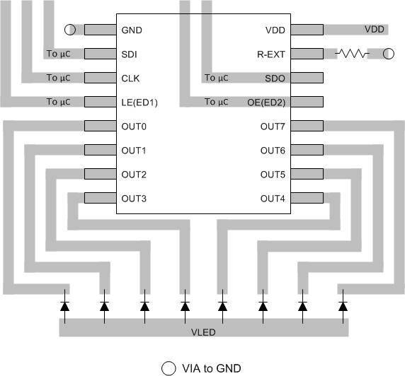 Figure 24. PW Package Layout
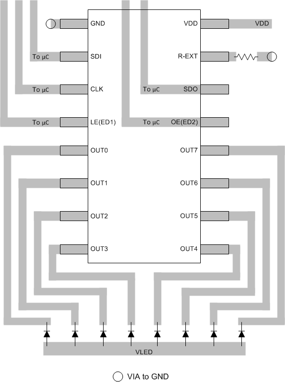 Figure 25. D Package Layout