SLVS695D June 2007 – January 2015 TLC5916 , TLC5917
PRODUCTION DATA.
- 1 Features
- 2 Applications
- 3 Description
- 4 Revision History
- 5 Device Comparison Table
- 6 Pin Configuration and Functions
-
7 Specifications
- 7.1 Absolute Maximum Ratings
- 7.2 ESD Ratings
- 7.3 Recommended Operating Conditions
- 7.4 Thermal Information
- 7.5 Electrical Characteristics: VDD = 3 V
- 7.6 Electrical Characteristics: VDD = 5.5 V
- 7.7 Switching Characteristics: VDD = 3 V
- 7.8 Switching Characteristics: VDD = 5.5 V
- 7.9 Timing Requirements
- 7.10 Typical Characteristics
- 8 Parameter Measurement Information
- 9 Detailed Description
- 10Application and Implementation
- 11Power Supply Recommendations
- 12Layout
- 13Device and Documentation Support
- 14Mechanical, Packaging, and Orderable Information
Package Options
Mechanical Data (Package|Pins)
Thermal pad, mechanical data (Package|Pins)
Orderable Information
6 Pin Configuration and Functions
16-PIN
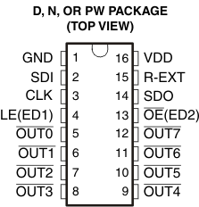
Pin Functions
| PIN | I/O | DESCRIPTION | |
|---|---|---|---|
| NAME | NO. | ||
| CLK | 3 | I | Clock input for data shift on rising edge |
| GND | 1 | – | Ground for control logic and current sink |
| LE(ED1) | 4 | I | Data strobe input Serial data is transferred to the respective latch when LE(ED1) is high. The data is latched when LE(ED1) goes low. Also, a control signal input for an Error Detection Mode and Current Adjust Mode (see Timing Diagram). LE(ED1) has an internal pulldown. |
| OE(ED2) | 13 | I | Output enable. When OE(ED2) is active (low), the output drivers are enabled; when OE(ED2) is high, all output drivers are turned OFF (blanked). Also, a control signal input for an Error Detection Mode and Current Adjust Mode (see Figure 11). OE(ED2) has an internal pullup. |
| OUT0 to OUT7 | 5 to 12 | O | Constant-current outputs |
| R-EXT | 15 | I | External Resistor - Connect an external resistor to ground to set the current for all outputs |
| SDI | 2 | I | Serial-data input to the Shift register |
| SDO | 14 | O | Serial-data output to the following SDI of next driver IC or to the microcontroller |
| VDD | 16 | I | Supply voltage |