SBVS146D August 2010 – December 2015 TLC5971
PRODUCTION DATA.
- 1 Features
- 2 Applications
- 3 Description
- 4 Revision History
- 5 Pin Configuration and Functions
- 6 Specifications
- 7 Parametric Measurement Information
-
8 Detailed Description
- 8.1 Overview
- 8.2 Functional Block Diagram
- 8.3 Feature Description
- 8.4 Device Functional Modes
- 8.5 Programming
- 9 Application and Implementation
- 10Power Supply Recommendations
- 11Layout
- 12Device and Documentation Support
- 13Mechanical, Packaging, and Orderable Information
Package Options
Mechanical Data (Package|Pins)
Thermal pad, mechanical data (Package|Pins)
Orderable Information
1 Features
- 12 Constant-Current Sink Output Channels
- Current Capability: 60 mA Per Channel
- Grayscale (GS) Control With Enhanced Spectrum PWM:
16-Bit (65536 Steps) -
Global Brightness Control (BC):
7-Bit (128 Steps) for Each Color Group - Power-Supply Voltage Range:
- Internal Linear Regulator: 6 V to 17 V
- Direct Power Supply: 3 V to 5.5 V
- LED Supply Voltage: Up to 17 V
- Constant-Current Accuracy:
- Channel-to-Channel = ±1% (Typical)
- Device-to-Device = ±1% (Typical)
- Data Transfer Rate: 20 MHz
- Linear Voltage Regulator: 3.3 V
- Auto Display Repeat Function
- Display Timing Reset Function
- Internal and External Selectable GS Clock
- Thermal Shutdown (TSD) With Auto Restart
- Unlimited Device Cascading
- Operating Temperature Range: –40°C to +85°C
2 Applications
RGB LED Cluster Lamp Displays
3 Description
The TLC5971 device is a 12-channel, constant-current sink driver. Each output channel has individually adjustable currents with 65536 PWM grayscale (GS) steps. Also, each color group can be controlled by 128 constant-current sink steps with the global brightness control (BC) function. GS control and BC are accessible through a two-wire signal interface. The maximum current value for each channel is set by a single external resistor. All constant-current outputs are turned off when the IC is in an overtemperature condition.
Device Information(1)
| PART NUMBER | PACKAGE | BODY SIZE (NOM) |
|---|---|---|
| TLC5971 | HTSSOP (20) | 6.50 mm × 4.40 mm |
| VQFN (24) | 4.00 mm × 4.00 mm |
- For all available packages, see the orderable addendum at the end of the data sheet.
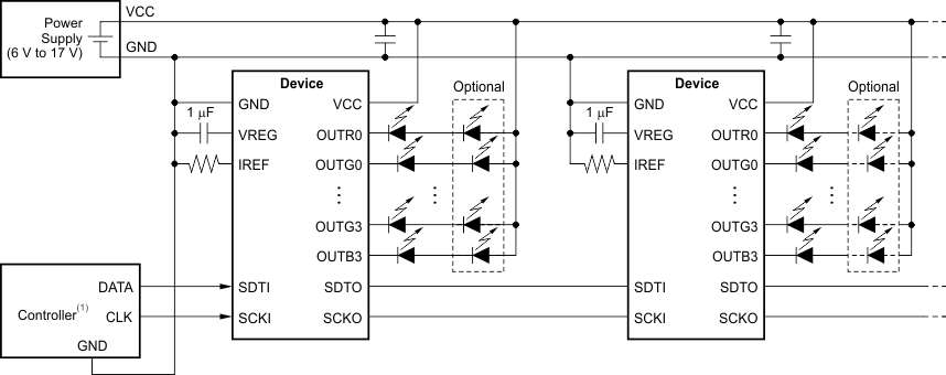
Typical Application Circuit Example (Internal Linear Regulator Using VCC = 6 V to 17 V)

1. The output voltage range is from 0 V to 3.3 V.
NOTE: The number of LEDs in series changes, depending on the VCC voltage.