SBOS754A March 2016 – March 2016 TLV2314 , TLV314 , TLV4314
PRODUCTION DATA.
- 1 Features
- 2 Applications
- 3 Description
- 4 Revision History
- 5 Device Comparison Table
- 6 Pin Configuration and Functions
- 7 Specifications
- 8 Detailed Description
- 9 Application and Implementation
- 10Power Supply Recommendations
- 11Layout
- 12Device and Documentation Support
- 13Mechanical, Packaging, and Orderable Information
Package Options
Mechanical Data (Package|Pins)
Thermal pad, mechanical data (Package|Pins)
- DGK|8
Orderable Information
1 Features
2 Applications
- White Goods
- Handheld Test Equipment
- Portable Blood Glucose Systems
- Remote Sensing
- Active Filters
- Industrial Automation
- Battery-Powered Electronics
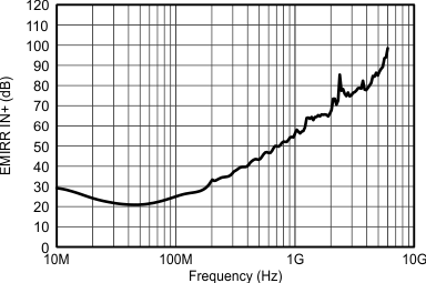
EMIRR vs Frequency

3 Description
The TLV314 family of single-, dual-, and quad-channel operational amplifiers represents a new generation of low-power, general-purpose operational amplifiers. Rail-to-rail input and output swings (RRIO), low quiescent current (150 μA typically at 5 V) combine with a wide bandwidth of 3 MHz to make this family very attractive for a variety of battery-powered applications that require a good balance between cost and performance. Additionally, the TLV314 family architecture achieves a low input bias current of 1 pA, allowing for applications with MΩ source impedances.
The robust design of the TLV314 devices provides ease-of-use to the circuit designer: unity-gain stability, RRIO, capacitive loads of up to 300 pF, an integrated RF/EMI rejection filter, no phase reversal in overdrive conditions, and high electrostatic discharge (ESD) protection (4-kV HBM).
These devices are optimized for low-voltage operation as low as 1.8 V (±0.9 V) and up to 5.5 V (±2.75 V), and are specified over the extended industrial temperature range of –40°C to +125°C.
The TLV314 (single) is available in both 5-pin SC70 and SOT-23 packages. The TLV2314 (dual) is offered in 8-pin SOIC and VSSOP packages. The quad-channel TLV4314 is offered in a 14-pin TSSOP package.
Device Information(1)
| PART NUMBER | PACKAGE | BODY SIZE (NOM) |
|---|---|---|
| TLV314 | SOT-23 (5) | 2.90 mm × 1.60 mm |
| SC70 (5) | 2.00 mm × 1.25 mm | |
| TLV2314 | VSSOP (8) | 3.00 mm × 3.00 mm |
| SOIC (8) | 4.90 mm × 3.91 mm | |
| TLV4314 | TSSOP (14) | 5.00 mm × 4.40 mm |
- For all available packages, see the orderable addendum at the end of the data sheet.