SLOS351E February 2004 – November 2016 TLV271 , TLV272 , TLV274
PRODUCTION DATA.
- 1 Features
- 2 Applications
- 3 Description
- 4 Revision History
- 5 Device Comparison Table
- 6 Pin Configuration and Functions
-
7 Specifications
- 7.1 Absolute Maximum Ratings
- 7.2 Recommended Operating Conditions
- 7.3 Thermal Information: TLV271
- 7.4 Thermal Information: TLV272
- 7.5 Thermal Information: TLV274
- 7.6 Electrical Characteristics: DC Characteristics
- 7.7 Electrical Characteristics: Input Characteristics
- 7.8 Electrical Characteristics: Output Characteristics
- 7.9 Electrical Characteristics: Power Supply
- 7.10 Electrical Characteristics: Dynamic Performance
- 7.11 Electrical Characteristics: Noise/Distortion Performance
- 7.12 Typical Characteristics
- 8 Detailed Description
- 9 Application and Implementation
- 10Power Supply Recommendations
- 11Layout
- 12Device and Documentation Support
- 13Mechanical, Packaging, and Orderable Information
Package Options
Refer to the PDF data sheet for device specific package drawings
Mechanical Data (Package|Pins)
- D|8
- P|8
- DGK|8
Thermal pad, mechanical data (Package|Pins)
Orderable Information
9 Application and Implementation
NOTE
Information in the following applications sections is not part of the TI component specification, and TI does not warrant its accuracy or completeness. TI’s customers are responsible for determining suitability of components for their purposes. Customers should validate and test their design implementation to confirm system functionality.
9.1 Application Information
The TLV27x family offers outstanding DC and AC performance. These devices operate up to a 16-V power supply and offer ultra-low input bias current and 3-MHz bandwidth. These features make the TLV27x a robust operational amplifier for battery-powered and industrial applications.
9.2 Typical Application
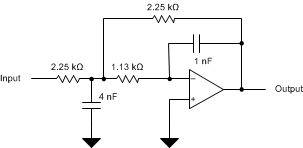 Figure 27. Second-Order, Low-Pass Filter
9.2.1 Design Requirements
- Gain = 1 V/V
- Low-pass cutoff frequency = 50 kHz
- –40-db/dec filter response
- Maintain less than 3-dB gain peaking in the gain versus frequency response
9.2.2 Detailed Design Procedure
The infinite-gain multiple-feedback circuit for a low-pass network function is shown in Figure 27. Use Equation 2 to calculate the voltage transfer function.

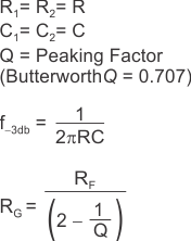
This circuit produces a signal inversion. For this circuit, the gain at DC and the low-pass cutoff frequency are calculated by Equation 3:

Software tools are readily available to simplify filter design. WEBENCH® Filter Designer is a simple, powerful, and easy-to-use active filter design program. The WEBENCH® Filter Designer lets you create optimized filter designs using a selection of TI operational amplifiers and passive components from TI's vendor partners.
Available as a web-based tool from the WEBENCH Design Center, WEBENCH Filter Designer allows you to design, optimize, and simulate complete multistage active filter solutions within minutes.
9.2.3 Application Curve
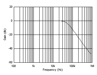 Figure 28. TLV27x Second-Order, 50-kHz, Low-Pass Filter
9.3 System Examples
9.3.1 General Configurations
When receiving low-level signals, limiting the bandwidth of the incoming signals into the system is often required. The simplest way to accomplish this limiting is to place an RC filter at the noninverting terminal of the amplifier (see Figure 29 and Equation 4).
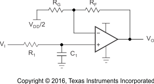 Figure 29. Single-Pole Low-Pass Filter

If even more attenuation is needed, a multiple pole filter is required. The Sallen-Key filter, shown in Figure 30, can be used for this task. For best results, the amplifier should have a bandwidth that is 8 to 10 times the filter frequency bandwidth; refer to Equation 5. Failure to use an amplifier with this characteristic can result in phase shift of the amplifier.
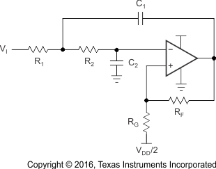 Figure 30. Two-Pole, Low-Pass, Sallen-Key Filter
