SBOS856A February 2017 – December 2017 TLV3201-Q1 , TLV3202-Q1
PRODUCTION DATA.
- 1 Features
- 2 Applications
- 3 Description
- 4 Revision History
- 5 Device Comparison Table
- 6 Pin Configuration and Functions
- 7 Specifications
- 8 Detailed Description
- 9 Application and Implementation
- 10Power Supply Recommendations
- 11Layout
- 12Device and Documentation Support
- 13Mechanical, Packaging, and Orderable Information
Package Options
Mechanical Data (Package|Pins)
- DGK|8
Thermal pad, mechanical data (Package|Pins)
- DGK|8
Orderable Information
1 Features
- Qualified for Automotive Applications
- AEC Q100-Qualified With the Following Results
- Device Temperature Grade 1: –40°C to +125°C Ambient Operating Temperature
- Device HBM ESD Classification Level 2 (TLV3201-Q1)
- Device HBM ESD Classification Level 3A (TLV3202-Q1)
- Device CDM ESD Classification Level C5
- Low Propagation Delay: 40 ns
- Low Quiescent Current:
40 µA per Channel - Input Common-Mode Range Extends 200 mV Beyond Either Rail
- Low Input Offset Voltage: 1 mV
- Push-Pull Outputs
- Supply Range: 2.7 V to 5.5 V
- Small Packages:
5-Pin SC70 and 8-Pin VSSOP
2 Applications
- Engine Control Units (ECU)
- Body Control Modules (BCM)
- Battery Management Systems (BMS)
- HEV/EV Inverter and Motor Control
- Ultrasonic Ranging and LIDAR
- Steering and Traction Controllers
- Occupant Detection
- Infotainment Systems
3 Description
The TLV3201-Q1 and TLV3202-Q1 are single and dual-channel comparators that offer the ultimate combination of high speed (40 ns) and low-power consumption (40 µA), both in extremely small packages with features such as rail-to-rail input, low offset voltage (1 mV), and large output drive current. The devices are also very easy to implement in a wide variety of applications where response time is critical.
The TLV320x-Q1 family is available in single (TLV3201-Q1) and dual (TLV3202-Q1) channel versions, both with push-pull outputs. The TLV3201-Q1 is available in the 5-pin SC70 package. The TLV3202-Q1 is available in the 8-pin VSSOP package. All devices are specified for operation across the expanded industrial temperature range of –40°C to +125°C.
Device Information(1)
| PART NUMBER | PACKAGE | BODY SIZE (NOM) |
|---|---|---|
| TLV3201-Q1 | SC70 (5) | 2.00 mm × 1.25 mm |
| TLV3202-Q1 | VSSOP (8) | 3.00 mm × 3.00 mm |
- For all available packages, see the orderable addendum at the end of the data sheet.
space
space
space
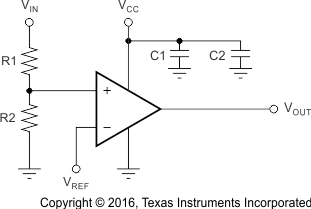
Threshold Detector

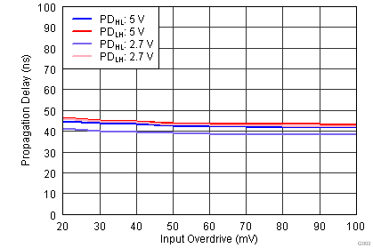
Propagation Delay vs. Overdrive
