SLAS671C February 2010 – January 2017 TLV320DAC3100
PRODUCTION DATA.
- 1 Device Overview
- 2 Revision History
- 3 Pin Configuration and Functions
-
4 Specifications
- 4.1 Absolute Maximum Ratings
- 4.2 ESD Ratings
- 4.3 Recommended Operating Conditions
- 4.4 Thermal Information
- 4.5 Electrical Characteristics
- 4.6 Power Dissipation Ratings
- 4.7 I2S, LJF, and RJF Timing in Master Mode
- 4.8 I2S, LJF, and RJF Timing in Slave Mode
- 4.9 DSP Timing in Master Mode
- 4.10 DSP Timing in Slave Mode
- 4.11 I2C Interface Timing
- 4.12 Typical Characteristics
- 5 Parameter Measurement Information
-
6 Detailed Description
- 6.1 Overview
- 6.2 Functional Block Diagram
- 6.3
Feature Description
- 6.3.1 Power-Supply Sequence
- 6.3.2 Reset
- 6.3.3 Device Start-Up Lockout Times
- 6.3.4 PLL Start-Up
- 6.3.5 Power-Stage Reset
- 6.3.6 Software Power Down
- 6.3.7 Audio Analog I/O
- 6.3.8
Digital Processing Low-Power Modes
- 6.3.8.1 DAC Playback on Headphones, Stereo, 48 kHz, DVDD = 1.8 V, AVDD = 3.3 V, HPVDD = 3.3 V
- 6.3.8.2 DAC Playback on Headphones, Mono, 48 kHz, DVDD = 1.8 V, AVDD = 3.3 V, HPVDD = 3.3 V
- 6.3.8.3 DAC Playback on Headphones, Stereo, 8 kHz, DVDD = 1.8 V, AVDD = 3.3 V, HPVDD = 3.3 V
- 6.3.8.4 DAC Playback on Headphones, Mono, 8 kHz, DVDD = 1.8 V, AVDD = 3.3 V, HPVDD = 3.3 V
- 6.3.8.5 DAC Playback on Headphones, Stereo, 192 kHz, DVDD = 1.8 V, AVDD = 3.3 V, HPVDD = 3.3 V
- 6.3.8.6 DAC Playback on Line Out (10 k-Ω load), Stereo, 48 kHz, DVDD = 1.8 V, AVDD = 3 V, HPVDD = 3 V
- 6.3.9 Analog Signals
- 6.3.10
Audio DAC and Audio Analog Outputs
- 6.3.10.1
DAC
- 6.3.10.1.1 DAC Processing Blocks
- 6.3.10.1.2
DAC Processing Blocks — Details
- 6.3.10.1.2.1 Three Biquads, Filter A
- 6.3.10.1.2.2 Six Biquads, First-Order IIR, DRC, Filter A or B
- 6.3.10.1.2.3 Six Biquads, First-Order IIR, Filter A or B
- 6.3.10.1.2.4 IIR, Filter B or C
- 6.3.10.1.2.5 Four Biquads, DRC, Filter B
- 6.3.10.1.2.6 Four Biquads, Filter B
- 6.3.10.1.2.7 Four Biquads, First-Order IIR, DRC, Filter C
- 6.3.10.1.2.8 Four Biquads, First-Order IIR, Filter C
- 6.3.10.1.2.9 Two Biquads, 3D, Filter A
- 6.3.10.1.2.10 Five Biquads, DRC, 3D, Filter A
- 6.3.10.1.2.11 Five Biquads, DRC, 3D, Beep Generator, Filter A
- 6.3.10.1.3 DAC User-Programmable Filters
- 6.3.10.1.4 DAC Interpolation Filter Characteristics
- 6.3.10.2 DAC Digital-Volume Control
- 6.3.10.3 Volume Control Pin
- 6.3.10.4 Dynamic Range Compression
- 6.3.10.5 Headphone Detection
- 6.3.10.6 Interrupts
- 6.3.10.7 Key-Click Functionality With Digital Sine-Wave Generator (PRB_P25)
- 6.3.10.8 Programming DAC Digital Filter Coefficients
- 6.3.10.9 Updating DAC Digital Filter Coefficients During PLAY
- 6.3.10.10 Digital Mixing and Routing
- 6.3.10.11 Analog Audio Routing
- 6.3.10.12 Analog Outputs
- 6.3.10.13 Audio-Output Stage-Power Configurations
- 6.3.10.14 DAC Setup
- 6.3.10.15 Example Register Setup to Play Digital Data Through DAC and Headphone/Speaker Outputs
- 6.3.10.1
DAC
- 6.3.11 CLOCK Generation and PLL
- 6.3.12 Timer
- 6.3.13 Digital Audio and Control Interface
- 6.4
Register Map
- 6.4.1 TLV320DAC3100 Register Map
- 6.4.2
Registers
- 6.4.2.1 Control Registers, Page 0 (Default Page): Clock Multipliers, Dividers, Serial Interfaces, Flags, Interrupts, and GPIOs
- 6.4.2.2 Control Registers, Page 1: DAC, Power-Controls, and MISC Logic-Related Programmability
- 6.4.2.3 Control Registers, Page 3: MCLK Divider for Programmable Delay Timer
- 6.4.2.4 Control Registers, Page 8: DAC Programmable Coefficients RAM Buffer A (1:63)
- 6.4.2.5 Control Registers, Page 9: DAC Programmable Coefficients RAM Buffer A (65:127)
- 6.4.2.6 Control Registers, Page 12: DAC Programmable Coefficients RAM Buffer B (1:63)
- 6.4.2.7 Control Registers, Page 13: DAC Programmable Coefficients RAM Buffer B (65:127)
- 7 Application and Implementation
- 8 Power Supply Recommendations
- 9 Layout
- 10Device and Documentation Support
- 11Mechanical Packaging and Orderable Information
Package Options
Mechanical Data (Package|Pins)
- RHB|32
Thermal pad, mechanical data (Package|Pins)
- RHB|32
Orderable Information
4 Specifications
4.1 Absolute Maximum Ratings
over operating free-air temperature range (unless otherwise noted) (1)| MIN | MAX | UNIT | ||
|---|---|---|---|---|
| AVDD to AVSS | –0.3 | 3.9 | V | |
| DVDD to DVSS | –0.3 | 2.5 | V | |
| HPVDD to HPVSS | –0.3 | 3.9 | V | |
| SPKVDD to SPKVSS | –0.3 | 6 | V | |
| IOVDD to IOVSS | –0.3 | 3.9 | V | |
| Digital input voltage | IOVSS – 0.3 | IOVDD + 0.3 | V | |
| Analog input voltage | AVSS – 0.3 | AVDD + 0.3 | V | |
| Operating temperature | –40 | 85 | °C | |
| Junction temperature (TJ Max) | 105 | °C | ||
| Storage temperature, Tstg | –55 | 150 | °C | |
(1) Stresses beyond those listed under Absolute Maximum Ratings may cause permanent damage to the device. These are stress ratings only, and functional operation of the device at these or any other conditions beyond those indicated under Recommended Operating Conditions is not implied. Exposure to absolute-maximum-rated conditions for extended periods may affect device reliability.
4.2 ESD Ratings
| VALUE | UNIT | |||
|---|---|---|---|---|
| V(ESD) | Electrostatic discharge | Human-body model (HBM), per ANSI/ESDA/JEDEC JS-001(1) | ±2000 | V |
| Charged-device model (CDM), per JEDEC specification JESD22-C101(2) | ±1000 | |||
(1) JEDEC document JEP155 states that 500-V HBM allows safe manufacturing with a standard ESD control process.
(2) JEDEC document JEP157 states that 250-V CDM allows safe manufacturing with a standard ESD control process.
4.3 Recommended Operating Conditions
over operating free-air temperature range (unless otherwise noted)| MIN | NOM | MAX | UNIT | |||
|---|---|---|---|---|---|---|
| AVDD(2) | Power-supply voltage | Referenced to AVSS(1) | 2.7 | 3.3 | 3.6 | V |
| DVDD | Referenced to DVSS(1) | 1.65 | 1.8 | 1.95 | ||
| HPVDD | Referenced to HPVSS(1) | 2.7 | 3.3 | 3.6 | ||
| SPKVDD(2) | Referenced to SPKVSS(1) | 2.7 | 5.5 | |||
| IOVDD | Referenced to IOVSS(1) | 1.1 | 3.3 | 3.6 | ||
| Speaker impedance | Resistance applied across class-D ouput pins (BTL) | 4 | Ω | |||
| Headphone impedance | AC coupled to RL | 16 | Ω | |||
| VI | Analog audio full-scale input voltage | AVDD = 3.3 V, single-ended | 0.707 | VRMS | ||
| Stereo line output load impedance | AC coupled to RL | 10 | kΩ | |||
| MCLK(3) | Master clock frequency | IOVDD = 3.3 V | 50 | MHz | ||
| fSCL | SCL clock frequency | 400 | kHz | |||
| TA | Operating free-air temperature | –40 | 85 | °C | ||
(1) All grounds on board are tied together, so they should not differ in voltage by more than 0.2-V maximum for any combination of ground signals. By use of a wide trace or ground plane, ensure a low-impedance connection between HPVSS and DVSS.
(2) To minimize battery-current leakage, the SPKVDD voltage level should not be below the AVDD voltage level.
(3) The maximum input frequency must be 50 MHz for any digital pin used as a general-purpose clock.
4.4 Thermal Information
| THERMAL METRIC(1) | TLV320DAC3100 | UNIT | |
|---|---|---|---|
| RHB (VQFN) | |||
| 32 PINS | |||
| RθJA | Junction-to-ambient thermal resistance | 31.4 | °C/W |
| RθJC(top) | Junction-to-case (top) thermal resistance | 21.9 | °C/W |
| RθJB | Junction-to-board thermal resistance | 5.6 | °C/W |
| ψJT | Junction-to-top characterization parameter | 0.2 | °C/W |
| ψJB | Junction-to-board characterization parameter | 5.6 | °C/W |
| RθJC(bot) | Junction-to-case (bottom) thermal resistance | 0.9 | °C/W |
(1) For more information about traditional and new thermal metrics, see the Semiconductor and IC Package Thermal Metrics application report..
4.5 Electrical Characteristics
At 25°C, AVDD = HPVDD = IOVDD = 3.3 V, SPKVDD = 3.6 V, DVDD = 1.8 V, fS (audio) = 48 kHz, CODEC_CLKIN = 256 × fS, PLL = Off, VOL/MICDET pin disabled (unless otherwise noted)| PARAMETER | TEST CONDITIONS | MIN | TYP | MAX | UNIT | |
|---|---|---|---|---|---|---|
| INTERNAL OSCILLATOR-RC_CLK | ||||||
| Oscillator frequency | 8.2 | MHz | ||||
| VOLUME CONTROL PIN (ADC); VOL/MICDET pin enabled | ||||||
| Input voltage range | VOL/MICDET pin configured as volume control (page 0 / register 116, bit D7 = 1 and page 0 / register 67, bit D7 = 0) | 0 | 0.5 x AVDD | V | ||
| Input capacitance | 2 | pF | ||||
| Volume control steps | 128 | Steps | ||||
| MICROPHONE BIAS | ||||||
| Voltage output | Page 1 / register 46, bits D1–D0 = 10 | 2.25 | 2.5 | 2.75 | V | |
| Page 1 / register 46, bits D1–D0 = 01 | 2 | |||||
| Voltage regulation | At 4-mA load current, page 1 / register 46, bits D1–D0 = 10 (MICBIAS = 2.5 V) | 5 | mV | |||
| At 4-mA load current, page 1 / register 46, bits D1–D0 = 01 (MICBIAS = 2 V) | 7 | |||||
| AUDIO DAC | ||||||
| DAC HEADPHONE OUTPUT, AC-coupled load = 16 Ω (single-ended), driver gain = 0 dB, parasitic capacitance = 30 pF | ||||||
| Full-scale output voltage (0 dB) | Output common-mode setting = 1.65 V | 0.707 | VRMS | |||
| SNR | Signal-to-noise ratio | Measured as idle-channel noise, A-weighted(1) (2) | 80 | 95 | dB | |
| THD | Total harmonic distortion | 0-dBFS input | –85 | –65 | dB | |
| THD+N | Total harmonic distortion + noise | 0-dBFS input | –82 | –60 | dB | |
| Mute attenuation | 87 | dB | ||||
| PSRR | Power-supply rejection ratio(4) | Ripple on HPVDD (3.3 V) = 200 mVp-p at 1 kHz | –62 | dB | ||
| PO | Maximum output power | RL = 32 Ω, THD+N = –60 dB | 20 | mW | ||
| RL = 16 Ω, THD+N = –60 dB | 60 | |||||
| DAC LINEOUT (HP Driver in Lineout Mode) | ||||||
| SNR | Signal-to-noise ratio | Measured as idle-channel noise, A-weighted | 95 | dB | ||
| THD | Total harmonic distortion | 0-dBFS input, 0-dB gain | –86 | dB | ||
| THD+N | Total harmonic distortion + noise | 0-dBFS input, 0-dB gain | –82 | dB | ||
| DAC DIGITAL INTERPOLATION FILTER CHARACTERISTICS | ||||||
| See Section 6.3.10.1.4 for DAC interpolation filter characteristics. | ||||||
| DAC Output to Class-D SPEAKER OUTPUT; Load = 4 Ω (Differential), 50 pF | ||||||
| Output voltage | SPKVDD = 3.6 V, BTL measurement, DAC input = 0 dBFS, CM = 1.8 V, class-D gain = 6 dB, THD = –16.5 dB | 2.3 | VRMS | |||
| SPKVDD = 3.6 V, BTL measurement, DAC input = –2 dBFS, CM = 1.8 V, class-D gain = 6 dB, THD = –20 dB | 2.1 | |||||
| Output, common-mode | SPKVDD = 3.6 V, BTL measurement, DAC input = mute, class-D gain = 6 dB | 1.8 | V | |||
| SNR | Signal-to-noise ratio | SPKVDD = 3.6 V, BTL measurement, class-D gain = 6 dB, measured as idle-channel noise, A-weighted (with respect to full-scale output value of 2.3 VRMS)(1) (2) | 88 | dB | ||
| THD | Total harmonic distortion | SPKVDD = 3.6 V, BTL measurement, DAC input = –6 dBFS, CM = 1.8 V, class-D gain = 6 dB | –65 | dB | ||
| THD+N | Total harmonic distortion + noise | SPKVDD = 3.6 V, BTL measurement, DAC input = –6 dBFS, CM = 1.8 V, class-D gain = 6 dB | –63 | dB | ||
| PSRR | Power-supply rejection ratio(3) | SPKVDD = 3.6 V, BTL measurement, ripple on SPKVDD = 200 mVp-p at 1 kHz | –44 | dB | ||
| Mute attenuation | 110 | dB | ||||
| PO | Maximum output power | SPKVDD = 3.6 V, BTL measurement, CM = 1.8 V, class-D gain = 18 dB, THD = 10% | 1 | W | ||
| SPKVDD = 4.3 V, BTL measurement, CM = 1.8 V, class-D gain = 18 dB, THD = 10% | 1.5 | W | ||||
| SPKVDD = 5.5 V, BTL measurement, CM = 1.8 V, class-D gain = 18 dB, THD = 10% | 2.5 | W | ||||
| DAC Output to Class-D Speaker Output; Load = 8 Ω (Differential), 50 pF | ||||||
| Output voltage | SPKVDD = 3.6 V, BTL measurement, DAC input = 0 dBFS, CM = 1.8 V, class-D gain = 6 dB, THD = –16.5 dB | 2.2 | VRMS | |||
| SPKVDD = 3.6 V, BTL measurement, DAC input = –2 dBFS, CM = 1.8 V, class-D gain = 6 dB, THD = –20 dB | 2.1 | VRMS | ||||
| Output, common-mode | SPKVDD = 3.6 V, BTL measurement, DAC input = mute, class-D gain = 6 dB | 1.8 | V | |||
| SNR | Signal-to-noise ratio | SPKVDD = 3.6 V, BTL measurement, class-D gain = 6 dB, measured as idle-channel noise, A-weighted (with respect to full-scale output value of 2.2 VRMS) | 87 | dB | ||
| THD | Total harmonic distortion | SPKVDD = 3.6 V, BTL measurement, DAC input = –6 dBFS, CM = 1.8 V, class-D gain = 6 dB | –67 | dB | ||
| THD+N | Total harmonic distortion + noise | SPKVDD = 3.6 V, BTL measurement, DAC input = –6 dBFS, CM = 1.8 V, class-D gain = 6 dB | –66 | dB | ||
| PSRR | Power-supply rejection ratio(3) | SPKVDD = 3.6 V, BTL measurement, ripple on SPKVDD = 200 mVp-p at 1 kHz | –44 | dB | ||
| Mute attenuation | 110 | dB | ||||
| PO | Maximum output power | SPKVDD = 3.6 V, BTL measurement, CM = 1.8 V, class-D gain = 18 dB, THD = 10% | 0.7 | W | ||
| SPKVDD = 4.3 V, BTL measurement, CM = 1.8 V, class-D gain = 18 dB, THD = 10% | 1 | |||||
| SPKVDD = 5.5 V, BTL measurement, CM = 1.8 V, class-D gain = 18 dB, THD = 10% | 1.6 | |||||
| Output-stage leakage current for direct battery connection | SPKVDD = 4.3 V, device is powered down (power-up-reset condition) | 80 | nA | |||
| DAC POWER CONSUMPTION | ||||||
| For DAC power consumption based on the selected processing block, see Section 6.3.8. | ||||||
| DIGITAL INPUT/OUTPUT | ||||||
| Logic family | CMOS | |||||
| VIH | Logic Level | IIH = 5 µA, IOVDD = 1.6 V | 0.7 × IOVDD | V | ||
| IIH = 5 µA, IOVDD = 1.6 V | IOVDD | |||||
| VIL | IIL = 5 µA, IOVDD = 1.6 V | –0.3 | 0.3 × IOVDD | |||
| IIL = 5 µA, IOVDD = 1.6 V | 0 | |||||
| VOH | IOH = 2 TTL loads | 0.8 × IOVDD | ||||
| VOL | IOL = 2 TTL loads | 0.1 × IOVDD | ||||
| Capacitive load | 10 | pF | ||||
(1) Ratio of output level with 1-kHz full-scale sine-wave input, to the output level with the inputs short-circuited, measured A-weighted over a 20-Hz to 20-kHz bandwidth using an audio analyzer.
(2) All performance measurements done with 20-kHz low-pass filter and, where noted, A-weighted filter. Failure to use such a filter may result in higher THD+N and lower SNR and dynamic range readings than shown in the Electrical Characteristics. The low-pass filter removes out-of-band noise, which, although not audible, may affect dynamic specification values.
(3) DAC to speaker-out PSRR is a differential measurement calculated as PSRR = 20 × log(∆VSPK(P + M) / ∆VSPKVDD) .
(4) DAC to headphone-out PSRR measurement is calculated as PSRR = 20 × log(∆VHPL / ∆VHPVDD).
4.6 Power Dissipation Ratings
This data was taken using 2-oz. (0,071-mm thick) trace and copper pad that is soldered to a JEDEC high-K, standard 4-layer 3-inch × 3-inch (7,62-cm × 7,62-cm) PCB.| Power Rating at 25°C | Derating Factor | Power Rating at 70°C | Power Rating at 85°C |
|---|---|---|---|
| 2.3 W | 28.57 mW/°C | 1 W | 0.6 W |
4.7 I2S, LJF, and RJF Timing in Master Mode
All specifications at 25°C, DVDD = 1.8 V. Note: All timing specifications are measured at characterization but not tested at final test. See Figure 4-1.| PARAMETER | IOVDD = 1.1 V | IOVDD = 3.3 V | UNIT | |||
|---|---|---|---|---|---|---|
| MIN | MAX | MIN | MAX | |||
| td(WS) | WCLK delay | 45 | 20 | ns | ||
| td(DO-WS) | WCLK to delay (for LJF mode only) | 45 | 20 | ns | ||
| td(DO-BCLK) | BCLK to delay | 45 | 20 | ns | ||
| ts(DI) | DIN setup | 8 | 6 | ns | ||
| th(DI) | DIN hold | 8 | 6 | ns | ||
| tr | Rise time | 25 | 10 | ns | ||
| tf | Fall time | 25 | 10 | ns | ||
4.8 I2S, LJF, and RJF Timing in Slave Mode
All specifications at 25°C, DVDD = 1.8 V. Note: All timing specifications are measured at characterization but not tested at final test. See Figure 4-2.| PARAMETER | IOVDD = 1.1 V | IOVDD = 3.3 V | UNIT | |||
|---|---|---|---|---|---|---|
| MIN | MAX | MIN | MAX | |||
| tH(BCLK) | BCLK high period | 35 | 35 | ns | ||
| tL(BCLK) | BCLK low period | 35 | 35 | ns | ||
| ts(WS) | WCLK setup | 8 | 6 | ns | ||
| th(WS) | WCLK hold | 8 | 6 | ns | ||
| td(DO-WS) | WCLK to delay (for LJF mode only) | 45 | 20 | ns | ||
| td(DO-BCLK) | BCLK to delay | 45 | 20 | ns | ||
| ts(DI) | DIN setup | 8 | 6 | ns | ||
| th(DI) | DIN hold | 8 | 6 | ns | ||
| tr | Rise time | 4 | 4 | ns | ||
| tf | Fall time | 4 | 4 | ns | ||
4.9 DSP Timing in Master Mode
All specifications at 25°C, DVDD = 1.8 V. Note: All timing specifications are measured at characterization but not tested at final test. See Figure 4-3.| PARAMETER | IOVDD = 1.1 V | IOVDD = 3.3 V | UNIT | |||
|---|---|---|---|---|---|---|
| MIN | MAX | MIN | MAX | |||
| td(WS) | WCLK delay | 45 | 20 | ns | ||
| td(DO-BCLK) | BCLK to delay | 45 | 20 | ns | ||
| ts(DI) | DIN setup | 8 | 8 | ns | ||
| th(DI) | DIN hold | 8 | 8 | ns | ||
| tr | Rise time | 25 | 10 | ns | ||
| tf | Fall time | 25 | 10 | ns | ||
4.10 DSP Timing in Slave Mode
All specifications at 25°C, DVDD = 1.8 V. Note: All timing specifications are measured at characterization but not tested at final test. See Figure 4-4.| PARAMETER | IOVDD = 1.1 V | IOVDD = 3.3 V | UNIT | |||
|---|---|---|---|---|---|---|
| MIN | MAX | MIN | MAX | |||
| tH(BCLK) | BCLK high period | 35 | 35 | ns | ||
| tL(BCLK) | BCLK low period | 35 | 35 | ns | ||
| ts(WS) | WCLK setup | 8 | 8 | ns | ||
| th(WS) | WCLK hold | 8 | 8 | ns | ||
| td(DO-BCLK) | BCLK to delay | 45 | 20 | ns | ||
| ts(DI) | DIN setup | 8 | 8 | ns | ||
| th(DI) | DIN hold | 8 | 8 | ns | ||
| tr | Rise time | 4 | 4 | ns | ||
| tf | Fall time | 4 | 4 | ns | ||
4.11 I2C Interface Timing
All specifications at 25°C, DVDD = 1.8 V. Note: All timing specifications are measured at characterization.See Figure 4-5.| PARAMETER | Standard Mode | Fast Mode | UNIT | |||||
|---|---|---|---|---|---|---|---|---|
| MIN | TYP | MAX | MIN | TYP | MAX | |||
| fSCL | SCL clock frequency | 0 | 100 | 0 | 400 | kHz | ||
| tHD;STA | Hold time (repeated) START condition. After this period, the first clock pulse is generated. | 4 | 0.8 | μs | ||||
| tLOW | LOW period of the SCL clock | 4.7 | 1.3 | μs | ||||
| tHIGH | HIGH period of the SCL clock | 4 | 0.6 | μs | ||||
| tSU;STA | Setup time for a repeated START condition | 4.7 | 0.8 | μs | ||||
| tHD;DAT | Data hold time: for I2C bus devices | 0 | 3.45 | 0 | 0.9 | μs | ||
| tSU;DAT | Data set-up time | 250 | 100 | ns | ||||
| tr | SDA and SCL rise time | 1000 | 20 + 0.1Cb | 300 | ns | |||
| tf | SDA and SCL fall time | 300 | 20 + 0.1Cb | 300 | ns | |||
| tSU;STO | Set-up time for STOP condition | 4 | 0.8 | μs | ||||
| tBUF | Bus free time between a STOP and START condition | 4.7 | 1.3 | μs | ||||
| Cb | Capacitive load for each bus line | 400 | 400 | pF | ||||
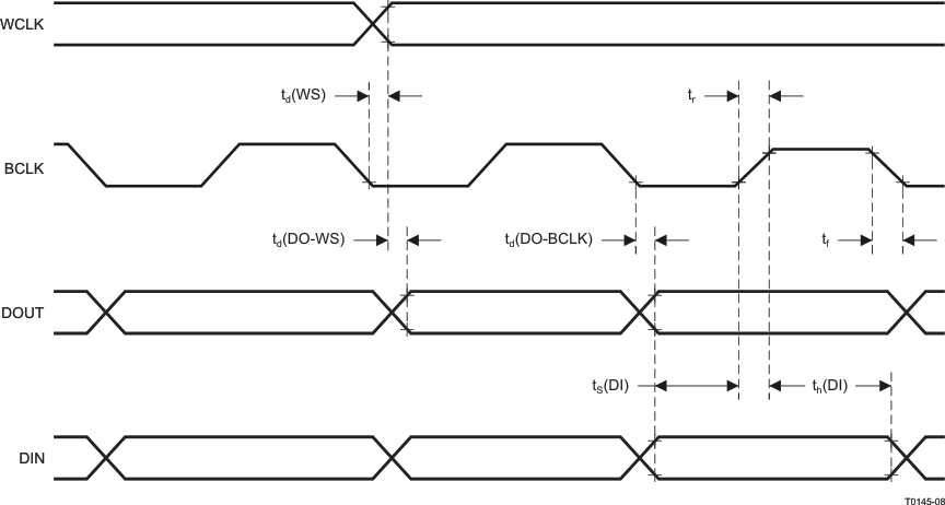 Figure 4-1 I2S/LJF/RJF Timing in Master Mode
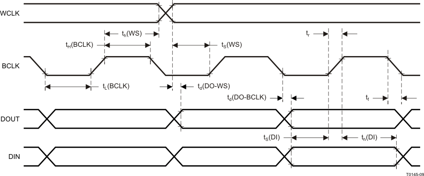 Figure 4-2 I2S/LJF/RJF Timing in Slave Mode
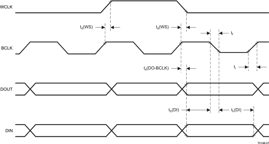 Figure 4-3 DSP Timing in Master Mode
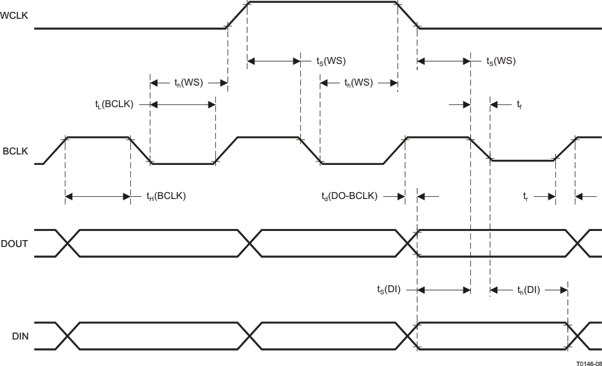 Figure 4-4 DSP Timing in Slave Mode
 Figure 4-5 I2C Interface Timing Diagram
4.12 Typical Characteristics
4.12.1 DAC Performance
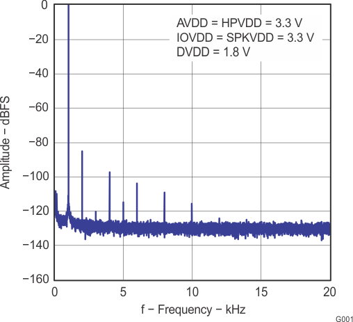 Figure 4-6 Amplitude vs Frequency
FFT - DAC to Line Output
TEXT ADDED FOR SPACING
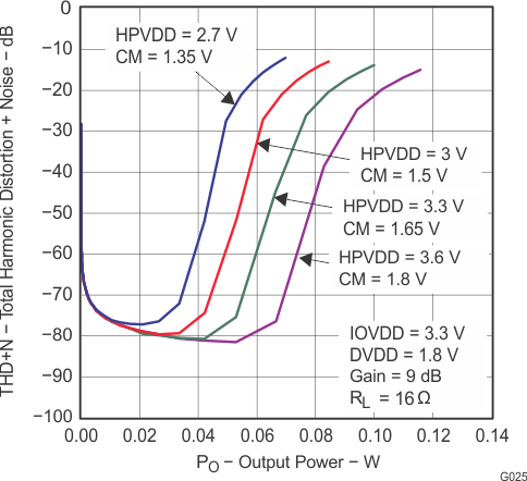 Figure 4-8 Total Harmonic Distortion + Noise vs Output Power
Headphone Output Power
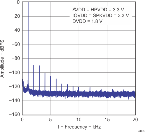 Figure 4-7 Amplitude vs Frequency
FFT - DAC to Headphone Output
TEXT ADDED FOR SPACING
4.12.2 Class-D Speaker Driver Performance
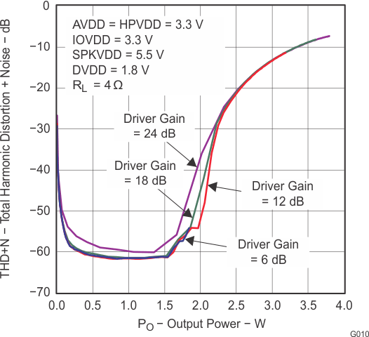 Figure 4-9 Total Harmonic Distortion + Noise vs Output Power
Max Class-D Speaker-Driver Output Power (RL = 4 Ω)
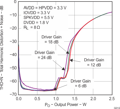 Figure 4-11 Total Harmonic Distortion + Noise vs Output Power
Max Class-D Speaker-Driver Output Power (RL = 8 Ω)
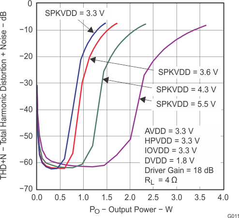 Figure 4-10 Total Harmonic Distortion + Noise vs Output Power
Class-D Speaker-Driver Output Power (RL = 4 Ω)
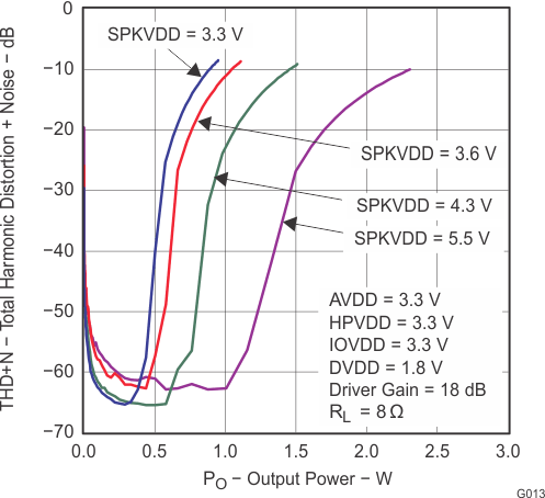 Figure 4-12 Total Harmonic Distortion + Noise vs Output Power
Class-D Speaker-Driver Output Power (RL = 8 Ω)
4.12.3 Analog Bypass Performance
H
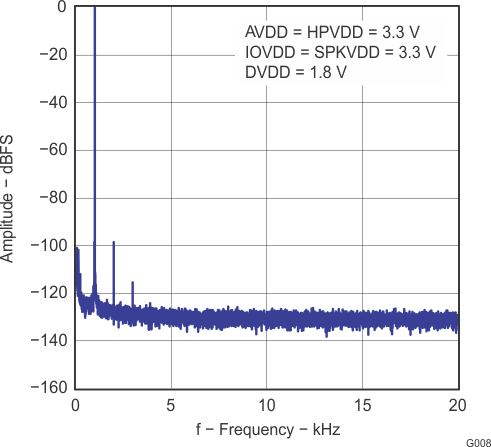 Figure 4-13 Amplitude vs Frequency
FFT - Line-In Bypass to Line Output
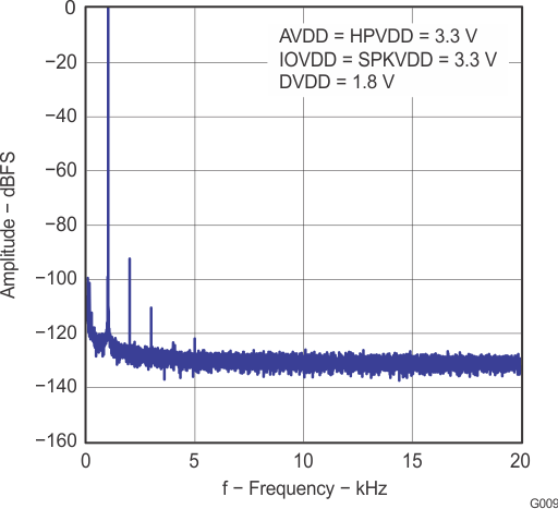 Figure 4-14 Amplitude vs Frequency
FFT - Line-In Bypass to Headphone Output
4.12.4 MICBIAS Performance
H
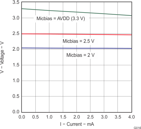 Figure 4-15 Voltage vs Current
MICBIAS