SNOSD27 May 2016 TLV522
PRODUCTION DATA.
- 1 Features
- 2 Applications
- 3 Description
- 4 Revision History
- 5 Pin Configuration and Functions
- 6 Specifications
- 7 Detailed Description
- 8 Application and Implementation
- 9 Power Supply Recommendations
- 10Layout
- 11Device and Documentation Support
- 12Mechanical, Packaging, and Orderable Information
Package Options
Mechanical Data (Package|Pins)
- DGK|8
Thermal pad, mechanical data (Package|Pins)
- DGK|8
Orderable Information
1 Features
- Unmatched Price Performance
- Wide Supply Range 1.7 V to 5.5 V
- Low Supply Current 500 nA
- Good Offset Voltage 4 mV (max)
- Good TcVos 1.5 µV/°C
- Gain-Bandwidth 8 kHz
- Rail-to-Rail Input and Output (RRIO)
- Unity-Gain Stable
- Low Input Bias Current 1 pA
- EMI Hardened
- Temperature Range –40°C to 125°C
- 8-pin VSSOP Package
2 Applications
- Personal Health Monitors
- Battery Packs
- Solar-Powered or Energy Harvested Systems
- PIR, Smoke, Gas, and Fire Detection Systems
- Battery Powered Internet of Things (IoT) Devices
- Remote Sensors/Wireless Sensing Nodes
- Wearables
- Glucose Monitoring
3 Description
The TLV522 500 nA dual, nanopower op amp offers optimum price performance in TI's nanopower family of operational amplifiers. The TLV522 provides 8 kHz of gain bandwidth from 500 nA of quiescent current, making it well suited for battery powered applications found in building automation and remote sensing nodes. Its CMOS input stage enables very low IBIAS, reducing errors commonly introduced in Megaohm feedback resistance topologies such as high-impedance photodiode and charge sense applications. Additionally, built-in EMI protection reduces sensitivity to unwanted RF signals from sources like mobile phones, WiFi, radio transmitters and RFID readers.
The TLV522 is offered in the 8-pin VSSOP (MSOP) package, and operates from –40°C to 125°C.
Device Information(1)
| PART NUMBER | PACKAGE | BODY SIZE (NOM) |
|---|---|---|
| TLV522 | VSSOP (8) | 3.00 mm x 3.00 mm |
- For all available packages, see the orderable addendum at the end of the data sheet.
space
space
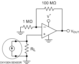
Nanopower Oxygen Sensor Amplifier
