SLVSAK9H October 2011 – January 2017 TLV62080 , TLV62084 , TLV62084A
UNLESS OTHERWISE NOTED, this document contains PRODUCTION DATA.
- 1 Features
- 2 Applications
- 3 Description
- 4 Revision History
- 5 Device Comparison Table
- 6 Pin Configuration and Functions
- 7 Specifications
- 8 Detailed Description
- 9 Application and Implementation
- 10Power Supply Recommendations
- 11Layout
- 12Device and Documentation Support
- 13Mechanical, Packaging, and Orderable Information
Package Options
Mechanical Data (Package|Pins)
- DSG|8
Thermal pad, mechanical data (Package|Pins)
- DSG|8
Orderable Information
9 Application and Implementation
NOTE
Information in the following applications sections is not part of the TI component specification, and TI does not warrant its accuracy or completeness. TI’s customers are responsible for determining suitability of components for their purposes. Customers should validate and test their design implementation to confirm system functionality.
9.1 Application Information
The devices are designed to operate from an input voltage supply range between 2.5 V (2.7 V for the TLV62084x devices) and 6 V with a maximum output current of 2 A (1.2 A for the TLV62080 device). The TLV6208x devices operate in PWM mode for medium to heavy load conditions and in power save mode at light load currents.
In PWM mode the TLV6208x converters operate with the nominal switching frequency of 2 MHz which provides a controlled frequency variation over the input voltage range. As the load current decreases, the converter enters power save mode, reducing the switching frequency and minimizing the IC quiescent current to achieve high efficiency over the entire load current range.
The WEBENCH software uses an iterative design procedure and accesses a comprehensive database of components when generating a design. See the Documentation Support section for additional documentation.
9.2 Typical Application
9.2.1 Design Requirements
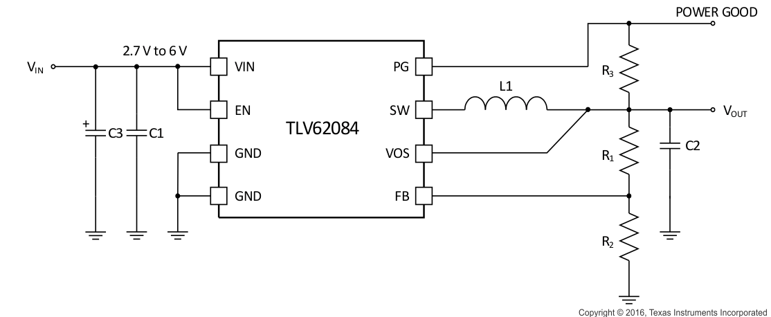
Use the following typical application design procedure to select external components values for the TLV62084 device.
Table 4. Design Parameters
| DESIGN PARAMETERS | EXAMPLE VALUES |
|---|---|
| Input Voltage Range | 2.8 V to 4.2 V |
| Output Voltage | 1.2 V |
| Transient Response | ±5% VOUT |
| Input Voltage Ripple | 400 mV |
| Output Voltage Ripple | 30 mV |
| Output Current Rating | 2 A |
| Operating frequency | 2 MHz |
9.2.2 Detailed Design Procedure
9.2.2.1 Custom Design With WEBENCH® Tools
Click here to create a custom design using the TLV62080 device with the WEBENCH® Power Designer.
- Start by entering the input voltage (VIN), output voltage (VOUT), and output current (IOUT) requirements.
- Optimize the design for key parameters such as efficiency, footprint, and cost using the optimizer dial.
- Compare the generated design with other possible solutions from Texas Instruments.
The WEBENCH Power Designer provides a customized schematic along with a list of materials with real-time pricing and component availability.
In most cases, these actions are available:
- Run electrical simulations to see important waveforms and circuit performance
- Run thermal simulations to understand board thermal performance
- Export customized schematic and layout into popular CAD formats
- Print PDF reports for the design, and share the design with colleagues
Get more information about WEBENCH tools at www.ti.com/WEBENCH.
Table 5. List of Components
| REFERENCE | DESCRIPTION | MANUFACTURER(1) |
|---|---|---|
| C1 | 10 μF, Ceramic Capacitor, 6.3 V, X5R, size 0603 | Std |
| C2 | 22 μF, Ceramic Capacitor, 6.3 V, X5R, size 0805, GRM21BR60J226ME39L | Murata |
| C3 | 47 μF, Tantalum Capacitor, 8 V, 35 mΩ, size 3528, T520B476M008ATE035 | Kemet |
| L1 | 1 μH, Power Inductor, 2.2 A, size 3 mm × 3 mm × 1.2 mm, XFL3012-102MEB | Coilcraft |
| R1 | 65.3 kΩ, Chip Resistor, 1/16 W, 1%, size 0603 | Std |
| R2 | 39.2 kΩ, Chip Resistor, 1/16 W, 1%, size 0603 | Std |
| R3 | 178 kΩ, Chip Resistor, 1/16 W, 1%, size 0603 | Std |
9.2.2.2 Output Filter Design
The inductor and the output capacitor together provide a low pass frequency filter. To simplify this process Table 6 outlines possible inductor and capacitor value combinations for the most application.
Table 6. Matrix of Output Capacitor and Inductor Combinations
| L [µH](3) | COUT [µF](3) | ||||
|---|---|---|---|---|---|
| 10 | 22 | 47 | 100 | 150 | |
| 0.47 | |||||
| 1 | + | +(1)(2) | + | + | |
| 2.2 | + | + | + | + | |
| 4.7 | |||||
9.2.2.3 Inductor Selection
The main parameter for the inductor selection is the inductor value and then the saturation current of the inductor. To calculate the maximum inductor current under static load conditions, Equation 2 is given.
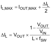
where
- IOUT,MAX = Maximum output current
- ΔIL = Inductor current ripple
- fSW = Switching frequency
- L = Inductor value
space
TI recommends choosing the saturation current for the inductor 20% to approximately 30% higher than the IL,MAX, out of Equation 2. A higher inductor value is also useful to lower ripple current, but increases the transient response time as well. The following inductors are recommended to be used in designs (see Table 7).
Table 7. List of Recommended Inductors
| INDUCTANCE [µH] |
CURRENT RATING [mA] |
DIMENSIONS L x W x H [mm3] |
DC RESISTANCE [mΩ typ] |
TYPE | MANUFACTURER(2) |
|---|---|---|---|---|---|
| 1 | 2500 | 3 × 3 × 1.2 | 35 | XFL3012-102ME | Coilcraft |
| 1 | 1650(1) | 3 × 3 × 1.2 | 40 | LQH3NPN1R0NJ0 | Murata |
| 2.2 | 2500 | 4 × 3.7 × 1.65 | 49 | LQH44PN2R2MP0 | Murata |
| 2.2 | 1600(1) | 3 × 3 × 1.2 | 81 | XFL3012-222ME | Coilcraft |
9.2.2.4 Capacitor Selection
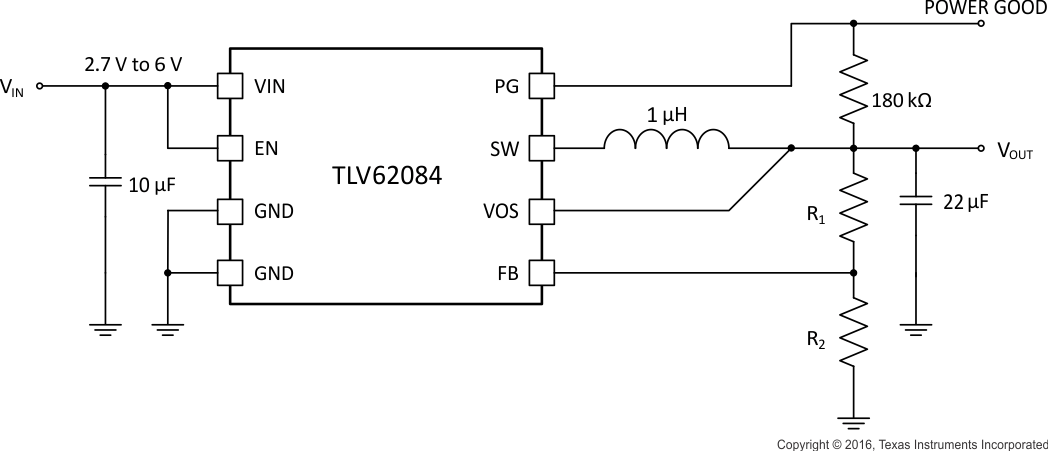
The input capacitor is the low impedance energy source for the converter which helps to provide stable operation. A low ESR multilayer ceramic capacitor is recommended for best filtering and must be placed between VIN and GND as close as possible to those terminals. For most applications 10 μF is sufficient though a larger value reduces input current ripple.
The architecture of the TLV6208x device allows use of tiny ceramic-type output capacitors with low equivalent-series resistance (ESR). These capacitors provide low output voltage ripple and are recommended. To keep the resistance up to high frequencies and to get narrow capacitance variation with temperature, TI recommends use of the X7R or X5R dielectric. The TLV62080 and TLV62084x devices are designed to operate with an output capacitance of 10 to 100 µF and beyond, as listed in Table 6. Load transient testing and measuring the bode plot are good ways to verify stability with larger capacitor values.
Table 8. List of Recommended Capacitors
| CAPACITANCE [µF] |
TYPE | DIMENSIONS L x W x H [mm3] |
MANUFACTURER(1) |
|---|---|---|---|
| 10 | GRM188R60J106M | 0603: 1.6 × 0.8 × 0.8 | Murata |
| 22 | GRM188R60G226M | 0603: 1.6 × 0.8 × 0.8 | Murata |
| 22 | GRM21BR60J226M | 0805: 2 × 1.2 × 1.25 | Murata |
9.2.2.5 Setting the Output Voltage
By selecting R1 and R2, the output voltage is programmed to the desired value. Use Equation 3 to calculate R1 and R2.
space

For best accuracy, R2 must be kept smaller than 40 kΩ to ensure that the current flowing through R2 is at least 100-times larger than IFB. Changing the sum towards a lower value increases the robustness against noise injection. Changing the sum towards higher values reduces the current consumption.
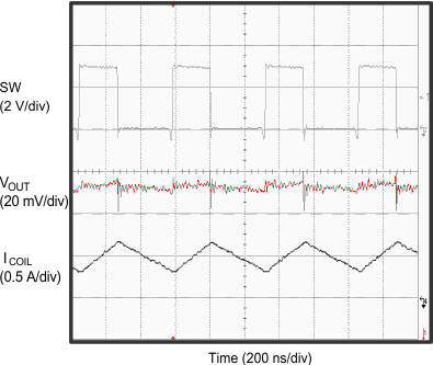
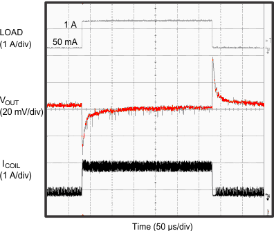
9.2.3 Application Curves
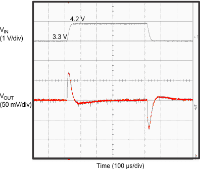
| VIN = 3.3 to 4.2 V | VOUT = 1.2 V | ILOAD = 2.2 Ω |
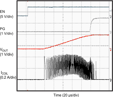
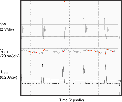
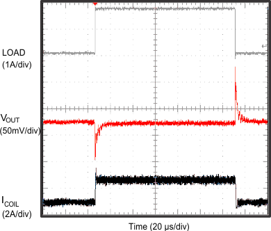
| VIN = 3.3 V | VOUT = 1.2 V | |
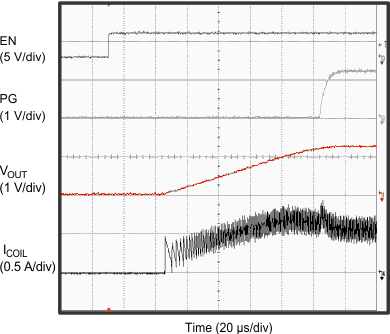
| VIN = 3.3 V | VOUT = 1.2 V | ILOAD = 2.2 Ω |
