SBVS151F December 2010 – April 2017 TLV705 , TLV705P
PRODUCTION DATA.
- 1 Features
- 2 Applications
- 3 Description
- 4 Revision History
- 5 Pin Configuration and Functions
- 6 Specifications
- 7 Detailed Description
- 8 Application and Implementation
- 9 Power Supply Recommendations
- 10Layout
- 11Device and Documentation Support
- 12Mechanical, Packaging, and Orderable Information
Package Options
Mechanical Data (Package|Pins)
Thermal pad, mechanical data (Package|Pins)
Orderable Information
7 Detailed Description
7.1 Overview
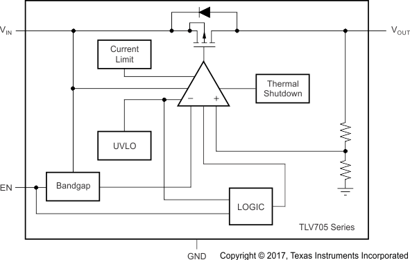
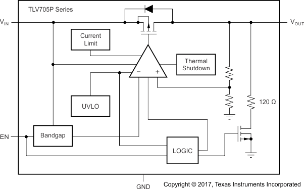
The TLV705 and TLV705P series of devices belong to a family of next-generation value low-dropout (LDO) voltage regulators. These devices consume low quiescent current and deliver excellent line and load transient performance. This performance, combined with low noise, very good PSRR with little (VIN – VOUT) headroom, makes these devices ideal for RF portable applications. This family of regulators offers sub-band-gap output voltages down to 0.7 V, current limit, and thermal protection, and are specified from –40°C to +125°C. The TLV705P provides an active pulldown circuit to quickly discharge the outputs.
7.3 Feature Description
7.3.1 Internal Current Limit
The internal current limits of the TLV705 series help protect the regulator during fault conditions. During current limit, the output sources a fixed amount of current that is largely independent of output voltage. In such a case, the output voltage is not regulated, and can be measured as VOUT = ILIMIT × RLOAD. The PMOS pass transistor dissipates [(VIN – VOUT) × ILIMIT] until a thermal shutdown is triggered and the device turns off. When the device cools down, the internal thermal shutdown circuit turns the device back on. If the fault condition continues, the device cycles between current limit and thermal shutdown; see Power Dissipation and Junction Temperature for more details.
The PMOS pass element in the TLV705 has a built-in body diode that conducts current when the voltage at VOUT exceeds the voltage at VIN. This current is not limited, so if extended reverse voltage operation is anticipated, TI recommends external limiting to 5% of the rated output current.
7.3.2 Undervoltage Lockout (UVLO)
The TLV705 uses an UVLO circuit to keep the output shut off until the internal circuitry is operating properly.
7.3.3 Start-Up Current
The TLV705 uses a unique start-up architecture that creates a constant start-up time regardless of the output capacitor. The start-up current is given by Equation 1. Equation 1 shows that start-up current is directly proportional to COUT.
The output voltage ramp rate is independent of COUT and the load current, and has a typical value of 0.06 V/μs.
The TLV705 automatically adjusts the soft-start current to supply both the load current and the current to charge COUT. For example, if ILOAD = 0 mA upon enabling the LDO, then ISTARTUP = 1 μF × 0.06 Vμs + 0 mA = 60 mA, which is the current that charges the output capacitor.
However, if ILOAD = 200 mA, then ISTARTUP = 1 μF × 0.06 V / μs + 200 mA = 260 mA, which is the required current to charge the output capacitor and supply the load current.
If the output capacitor and load increase such that the start-up current exceeds the output current limit, the start-up current is clamped at the typical current limit of 400 mA. For example, if COUT = 10 μF and
IOUT = 200 mA, then 10 μF × 0.06 V / μs + 200 mA = 800 mA is not supplied and is instead clamped at 400 mA.
7.3.4 Dropout Voltage
The TLV705 uses a PMOS pass transistor to achieve low dropout. When (VIN – VOUT) is less than the dropout voltage (VDO), the PMOS pass device is in the linear region of operation and the input-to-output resistance is the RDS(on) of the PMOS pass element. VDO approximately scales with the output current because the PMOS device functions as a resistor in dropout.
As with any linear regulator, PSRR and transient response are degraded as (VIN – VOUT) approaches dropout. This effect is shown in Figure 13 in the Typical Characteristics.
7.3.5 Shutdown
The enable pin (EN) is active high. The device is enabled when the EN pin goes above 0.9 V. This relatively lower value of voltage required to turn the LDO on can power the device with the GPIO of recent processors with a GPIO voltage lower than traditional microcontrollers. The device is turned off when the EN pin is held at less than 0.4 V. When shutdown capability is not required, EN can be connected to the VIN pin. The TLV705P version has internal active pulldown circuitry that discharges the output with a time constant of:
where
- RL = load resistance
- COUT = output capacitor
7.4 Device Functional Modes
7.4.1 Normal Operation
The device regulates to the nominal output voltage under the following conditions:
- The input voltage is greater than the nominal output voltage added to the dropout voltage.
- The output current is less than the current limit.
- The input voltage is greater than the UVLO voltage.
7.4.2 Dropout Operation
If the input voltage is lower than the nominal output voltage plus the specified dropout voltage, but all other conditions are met for normal operation, the device operates in dropout mode. In this condition, the output voltage is the same the input voltage minus the dropout voltage. The transient performance of the device is significantly degraded because the pass device is in a triode state and no longer regulates the output voltage of the LDO. Line or load transients in dropout can result in large output voltage deviations.
Table 1 lists the conditions that lead to the different modes of operation.
Table 1. Device Functional Mode Comparison
| OPERATING MODE | PARAMETER | |
|---|---|---|
| VIN | IOUT | |
| Normal mode | VIN > VOUT (nom) + VDO | IOUT < ICL |
| Dropout mode | VIN < VOUT (nom) + VDO | IOUT < ICL |
| Current limit | VIN > UVLO | IOUT > ICL |

