SBOS231I January 2002 – November 2015 TMP100 , TMP101
PRODUCTION DATA.
- 1 Features
- 2 Applications
- 3 Description
- 4 Revision History
- 5 Pin Configuration and Functions
- 6 Specifications
-
7 Detailed Description
- 7.1 Overview
- 7.2 Functional Block Diagram
- 7.3 Feature Description
- 7.4 Device Functional Modes
- 7.5 Programming
- 8 Application and Implementation
- 9 Power Supply Recommendations
- 10Layout
- 11Device and Documentation Support
- 12Mechanical, Packaging, and Orderable Information
Package Options
Mechanical Data (Package|Pins)
- DBV|6
Thermal pad, mechanical data (Package|Pins)
Orderable Information
7 Detailed Description
7.1 Overview
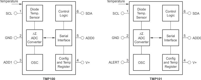
The TMP100 and TMP101 devices are digital temperature sensors optimal for thermal management and thermal protection applications. The TMP100 and TMP101 devices are Two-Wire, SMBus, and I2C interface-compatible. These devices are specified over a operating temperature range of −55°C to 125°C. The Functional Block Diagram section shows the internal block diagrams of the TMP100 and TMP101 devices.
The temperature sensor in the TMP100 and TMP101 devices is the chip itself. Thermal paths run through the package leads as well as the plastic package. The package leads provide the primary thermal path because of the lower thermal resistance of the metal. The GND pin of the TMP100 or TMP101 is directly connected to the metal lead frame, and is the best choice for thermal input.
7.2 Functional Block Diagram
7.3 Feature Description
7.3.1 Digital Temperature Output
The digital output from each temperature measurement conversion is stored in the read-only Temperature Register. The Temperature Register of the TMP100 or TMP101 device is a 12-bit, read-only register that stores the output of the most recent conversion. Two bytes must be read to obtain data and are listed in Table 6 and Table 7. The first 12 bits are used to indicate temperature with all the remaining bits equal to zero. The data format for temperature is listed in Table 1. Negative numbers are represented in binary twos complement format. Following power-up or reset, the temperature register reads 0°C until the first conversion is complete.
The user can obtain 9, 10, 11, or 12 bits of resolution by addressing the Configuration Register and setting the resolution bits accordingly. For 9-, 10-, or 11-bit resolution, the most significant bits (MSBs) in the Temperature Register are used with the unused least significant bits (LSBs) set to zero.
Table 1. Temperature Data Format
| TEMPERATURE (°C) |
DIGITAL OUTPUT | |
|---|---|---|
| BINARY | HEX | |
| 128 | 0111 1111 1111 | 7FF |
| 127.9375 | 0111 1111 1111 | 7FF |
| 100 | 0110 0100 0000 | 640 |
| 80 | 0101 0000 0000 | 500 |
| 75 | 0100 1011 0000 | 4B0 |
| 50 | 0011 0010 0000 | 320 |
| 25 | 0001 1001 0000 | 190 |
| 0.25 | 0000 0000 0100 | 004 |
| 0 | 0000 0000 0000 | 000 |
| –0.25 | 1111 1111 1100 | FFC |
| –25 | 1110 0111 0000 | E70 |
| –55 | 1100 1001 0000 | C90 |
| –128 | 1000 0000 0000 | 800 |
7.3.2 Serial Interface
The TMP100 and TMP101 devices operate only as slave devices on the SMBus, Two-Wire, and I2C interface-compatible bus. Connections to the bus are made through the open-drain I/O lines SDA and SCL. The TMP100 and TMP101 devices support the transmission protocol for fast (up to 400 kHz) and high-speed (up to 2 MHz) modes. All data bytes are transmitted MSB first.
7.3.2.1 Bus Overview
The device that initiates the transfer is called a master, and the devices controlled by the master are slaves. The bus must be controlled by a master device that generates the serial clock (SCL), controls the bus access, and generates the START and STOP conditions.
To address a specific device, a START condition is initiated, indicated by pulling the data line (SDA) from a HIGH to LOW logic level while SCL is HIGH. All slaves on the bus shift in the slave address byte, with the last bit indicating whether a read or write operation is intended. During the ninth clock pulse, the slave being addressed responds to the master by generating an Acknowledge and pulling SDA LOW.
Data transfer is then initiated and sent over eight clock pulses followed by an Acknowledge Bit. During data transfer, SDA must remain stable while SCL is HIGH because any change in SDA while SCL is HIGH is interpreted as a control signal.
When all data are transferred, the master generates a STOP condition indicated by pulling SDA from LOW to HIGH, while SCL is HIGH.
7.3.2.2 Serial Bus Address
To program the TMP100 and TMP101 devices, the master must first address slave devices through a slave address byte. The slave address byte consists of seven address bits and a direction bit indicating the intent of executing a read or write operation.
The TMP100 device features two address pins to allow up to eight devices to be addressed on a single I2C interface. Table 2 describes the pin logic levels used to properly connect up to eight devices. Float indicates the pin is left unconnected. The state of pins ADD0 and ADD1 is sampled on the first I2C bus communication and must be set before any activity on the interface.
Table 2. Address Pins and Slave Addresses for the TMP100
| ADD1 | ADD0 | SLAVE ADDRESS |
|---|---|---|
| 0 | 0 | 1001000 |
| 0 | Float | 1001001 |
| 0 | 1 | 1001010 |
| 1 | 0 | 1001100 |
| 1 | Float | 1001101 |
| 1 | 1 | 1001110 |
| Float | 0 | 1001011 |
| Float | 1 | 1001111 |
The TMP101 device features one address pin and an ALERT pin, allowing up to three devices to be connected per bus. Pin logic levels are described in Table 3. The address pins of the TMP100 and TMP101 devices are read after reset or in response to an I2C address acquire request. Following reading, the state of the address pins is latched to minimize power dissipation associated with detection.
Table 3. Address Pins and Slave Addresses for the TMP101
| ADD0 | SLAVE ADDRESS |
|---|---|
| 0 | 1001000 |
| Float | 1001001 |
| 1 | 1001010 |
7.3.2.3 Writing and Reading to the TMP100 and TMP101
Accessing a particular register on the TMP100 and TMP101 devices is accomplished by writing the appropriate value to the Pointer Register. The value for the Pointer Register is the first byte transferred after the I2C slave address byte with the R/W bit LOW. Every write operation to the TMP100 and TMP101 devices requires a value for the Pointer Register (see Figure 7).
When reading from the TMP100 and TMP101 devices, the last value stored in the Pointer Register by a write operation is used to determine which register is read by a read operation. To change the register pointer for a read operation, a new value must be written to the Pointer Register. This action is accomplished by issuing an I2C slave address byte with the R/W bit LOW, followed by the Pointer Register Byte. No additional data are required. The master can then generate a START condition and send the I2C slave address byte with the R/W bit HIGH to initiate the read command; see Figure 8 for details of this sequence. If repeated reads from the same register are desired, the Pointer Register bytes do not have to be continually sent because the TMP100 and TMP101 devices remember the Pointer Register value until that value is changed by the next write operation.
7.3.2.4 Slave Mode Operations
The TMP100 and TMP101 devices can operate as a slave receiver or slave transmitter.
7.3.2.4.1 Slave Receiver Mode
The first byte transmitted by the master is the slave address, with the R/W bit LOW. The TMP100 or TMP101 devices then acknowledges reception of a valid address. The next byte transmitted by the master is the Pointer Register. The TMP100 or TMP101 devices then acknowledges reception of the Pointer Register byte. The next byte or bytes are written to the register addressed by the Pointer Register. The TMP100 and TMP101 devices acknowledge reception of each data byte. The master can terminate data transfer by generating a START or STOP condition.
7.3.2.4.2 Slave Transmitter Mode
The first byte is transmitted by the master and is the slave address, with the R/W bit HIGH. The slave acknowledges reception of a valid slave address. The next byte is transmitted by the slave and is the most significant byte of the register indicated by the Pointer Register. The master acknowledges reception of the data byte. The next byte transmitted by the slave is the least significant byte. The master acknowledges reception of the data byte. The master can terminate data transfer by generating a Not-Acknowledge on reception of any data byte, or generating a START or STOP condition.
7.3.2.5 SMBus Alert Function
The TMP101 device supports the SMBus Alert function. When the TMP101 device is operating in Interrupt Mode (TM = 1), the ALERT pin of the TMP101 device can be connected as an SMBus Alert signal. When a master senses that an ALERT condition is present on the ALERT line, the master sends an SMBus Alert command (00011001) on the bus. If the ALERT pin of the TMP101 device is active, the TMP101 device acknowledges the SMBus Alert command and responds by returning its slave address on the SDA line. The eighth bit (LSB) of the slave address byte indicates if the temperature exceeding THIGH or falling below TLOW caused the ALERT condition. For POL = 0, this bit is LOW if the temperature is greater than or equal to THIGH. This bit is HIGH if the temperature is less than TLOW. The polarity of this bit is inverted if POL = 1; see Figure 9 for details of this sequence.
If multiple devices on the bus respond to the SMBus Alert command, arbitration during the slave address portion of the SMBus alert command determine which device clears its ALERT status. If the TMP101 device wins the arbitration, its ALERT pin becomes inactive at the completion of the SMBus Alert command. If the TMP101 loses the arbitration, its ALERT pin remains active.
The TMP100 device also responds to the SMBus ALERT command if its TM bit is set to 1. Because the device does not have an ALERT pin, the device must periodically poll the device by issuing an SMBus Alert command. If the TMP100 device generates an ALERT, the device acknowledges the SMBus Alert command and returns its slave address in the next byte.
7.3.2.6 General Call
The TMP100 and TMP101 devices respond to the I2C General Call address (0000000) if the eighth bit is 0. The device acknowledges the General Call address and responds to commands in the second byte. If the second byte is 00000100, the TMP100 and TMP101 devices latch the status of their address pins, but do not reset. If the second byte is 00000110, the TMP100 and TMP101 devices latch the status of their address pins and reset their internal registers.
7.3.2.7 High-Speed Mode
In order for the I2C bus to operate at frequencies above 400 kHz, the master device must issue an Hs-mode master code (00001XXX) as the first byte after a START condition to switch the bus to high-speed operation. The TMP100 and TMP101 devices do not acknowledge this byte as required by the I2C specification, but do switch their input filters on SDA and SCL and their output filters on SDA to operate in Hs-mode, allowing transfers at up to 2 MHz. After the Hs-mode master code is issued, the master transmits an I2C slave address to initiate a data transfer operation. The bus continues to operate in Hs-mode until a STOP condition occurs on the bus. Upon receiving the STOP condition, the TMP100 and TMP101 devices switch the input and output filter back to fast-mode operation.
7.3.2.8 POR (Power-On Reset)
The TMP100 and TMP101 devices both have on-chip, power-on reset circuits that reset the device to default settings when the device is powered on. This circuit activates when the power supply is less than 0.3 V for more than 100 ms. If the TMP100 and TMP101 devices are powered down by removing supply voltage from the device, but the supply voltage is not assured to be less than 0.3 V, TI recommends issuing a General Call reset command on the I2C interface bus to ensure that the TMP100 and TMP101 devices are completely reset.
7.3.3 Timing Diagrams
The TMP100 and TMP101 devices are Two-Wire, SMBUs, and I2C interface-compatible. Figure 6 to Figure 9 describe the various operations on the TMP100 and TMP101. The following list provides bus definitions. Parameters for Figure 6 are defined in the Timing Requirements section.
Bus Idle: Both SDA and SCL lines remain HIGH.
Start Data Transfer: A change in the state of the SDA line, from HIGH to LOW, while the SCL line is HIGH, defines a START condition. Each data transfer is initiated with a START condition.
Stop Data Transfer: A change in the state of the SDA line from LOW to HIGH while the SCL line is HIGH defines a STOP condition. Each data transfer is terminated with a repeated START or STOP condition.
Data Transfer: The number of data bytes transferred between a START and a STOP condition is not limited and is determined by the master device. The receiver acknowledges the transfer of data.
Acknowledge: Each receiving device, when addressed, is obliged to generate an Acknowledge bit. A device that acknowledges must pull down the SDA line during the Acknowledge clock pulse in such a way that the SDA line is stable LOW during the HIGH period of the Acknowledge clock pulse. Setup and hold times must be taken into account. On a master receive, the termination of the data transfer can be signaled by the master generating a Not-Acknowledge on the last byte that is transmitted by the slave.
 Figure 6. I2C Timing Diagram
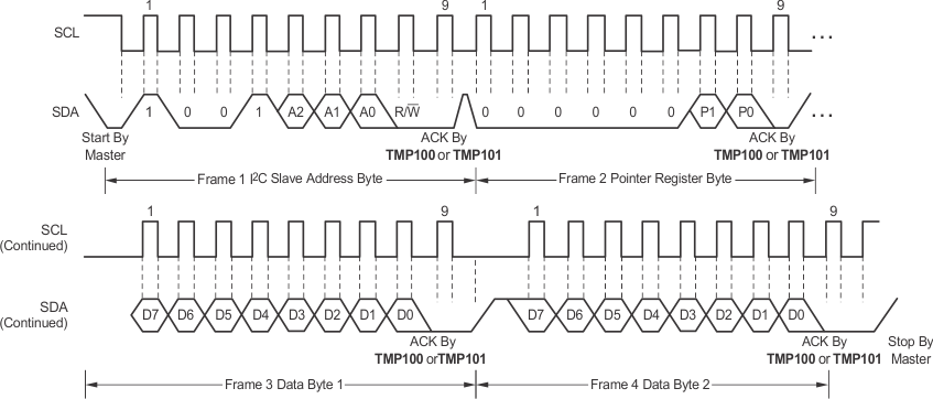 Figure 7. I2C Timing Diagram for Write Word Format
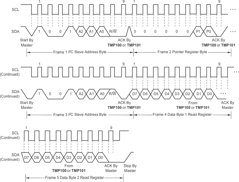 Figure 8. I2C Timing Diagram for Read Word Format
 Figure 9. Timing Diagram for SMBus ALERT
7.4 Device Functional Modes
7.4.1 Shutdown Mode (SD)
The Shutdown Mode of the TMP100 and TMP101 devices lets the user save maximum power by shutting down all device circuitry other than the serial interface, which reduces current consumption to less than 1 µA. For the TMP100 and TMP101 devices, Shutdown Mode is enabled when the SD bit is 1. The device shuts down when the current conversion is completed. For SD equal to 0, the device maintains continuous conversion.
7.4.2 OS/ALERT (OS)
The TMP100 and TMP101 devices feature a One-Shot Temperature Measurement Mode. When the device is in Shutdown Mode, writing 1 to the OS/ALERT bit starts a single temperature conversion. The device returns to the shutdown state at the completion of the single conversion. This feature is useful to reduce power consumption in the TMP100 and TMP101 devices when continuous monitoring of temperature is not required.
Reading the OS/ALERT bit provides information about the Comparator Mode status. The state of the POL bit inverts the polarity of data returned from the OS/ALERT bit. For POL = 0, the OS/ALERT reads as 1 until the temperature equals or exceeds THIGH for the programmed number of consecutive faults, causing the OS/ALERT bit to read as 0. The OS/ALERT bit continues to read as 0 until the temperature falls below TLOW for the programmed number of consecutive faults when the OS/ALERT bit again reads as 1. The status of the TM bit does not affect the status of the OS/ALERT bit.
7.4.3 Thermostat Mode (TM)
The Thermostat Mode bit of the TMP101 device indicates to the device whether to operate in Comparator Mode (TM = 0) or Interrupt Mode (TM = 1). For more information on comparator and interrupt modes, see the High- and Low-Limit Registers section.
7.4.3.1 Comparator Mode (TM = 0)
In Comparator Mode (TM = 0), the ALERT pin is activated when the temperature equals or exceeds the value in the THIGH register and remains active until the temperature falls below the value in the TLOW register. For more information on the Comparator Mode, see the High- and Low-Limit Registers section.
7.4.3.2 Interrupt Mode (TM = 1)
In Interrupt Mode (TM = 1), the ALERT pin is activated when the temperature exceeds THIGH or goes below the TLOW registers. The ALERT pin is cleared when the host controller reads the temperature register. For more information on the interrupt mode, see the High- and Low-Limit Registers section.
7.5 Programming
7.5.1 Pointer Register
Figure 10 shows the internal register structure of the TMP100 and TMP101 devices. The 8-bit Pointer Register of the TMP100 and TMP101 devices is used to address a given data register. The Pointer Register uses the two LSBs to identify which of the data registers respond to a read or write command. Table 4 identifies the bits of the Pointer Register byte. Table 5 describes the pointer address of the registers available in the TMP100 and TMP101 devices. The power-up reset value of P1 and P0 is 00.
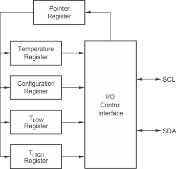 Figure 10. Internal Register Structure of the TMP100 and TMP101
7.5.1.1 Pointer Register Byte (pointer = N/A) [reset = 00h]
Table 4. Pointer Register Byte
| P7 | P6 | P5 | P4 | P3 | P2 | P1 | P0 |
|---|---|---|---|---|---|---|---|
| 0 | 0 | 0 | 0 | 0 | 0 | Register Bits | |
7.5.1.2 Pointer Addresses of the TMP100 and TMP101 Registers
Table 5. Pointer Addresses of the TMP100 and TMP101 Registers
| P1 | P0 | TYPE | REGISTER |
|---|---|---|---|
| 0 | 0 | R only, default | Temperature Register |
| 0 | 1 | R/W | Configuration Register |
| 1 | 0 | R/W | TLOW Register |
| 1 | 1 | R/W | THIGH Register |
7.5.2 Temperature Register
The Temperature Register of the TMP100 or TMP101 devices is a 12-bit, read-only register that stores the output of the most recent conversion. Two bytes must be read to obtain data, and are described in Table 6 and Table 7. The first 12 bits are used to indicate temperature, with all remaining bits equal to zero. Data format for temperature is summarized in Table 1. Following power-up or reset, the Temperature Register reads 0°C until the first conversion is complete.
Table 6. Byte 1 of the Temperature Register
| D7 | D6 | D5 | D4 | D3 | D2 | D1 | D0 |
|---|---|---|---|---|---|---|---|
| T11 | T10 | T9 | T8 | T7 | T6 | T5 | T4 |
Table 7. Byte 2 of the Temperature Register
| D7 | D6 | D5 | D4 | D3 | D2 | D1 | D0 |
|---|---|---|---|---|---|---|---|
| T3 | T2 | T1 | T0 | 0 | 0 | 0 | 0 |
7.5.3 Configuration Register
The Configuration Register is an 8-bit read and write register used to store bits that control the operational modes of the temperature sensor. Read and write operations are performed MSB-first. The format of the Configuration Register for the TMP100 and TMP101 devices is shown in Table 8, followed by a breakdown of the register bits. The power-up or reset value of the Configuration Register is all bits equal to 0. The OS/ALERT bit reads as 1 after power-up or reset value.
Table 8. Configuration Register Format
| BYTE | D7 | D6 | D5 | D4 | D3 | D2 | D1 | D0 |
|---|---|---|---|---|---|---|---|---|
| 1 | OS/ALERT | R1 | R0 | F1 | F0 | POL | TM | SD |
7.5.3.1 Shutdown Mode (SD)
The Shutdown Mode of the TMP100 and TMP101 devices allows the user to save maximum power by shutting down all device circuitry other than the serial interface, which reduces current consumption to less than 1 µA. For the TMP100 and TMP101 devices, Shutdown Mode is enabled when the SD bit is 1. The device shuts down when the current conversion is completed. For SD equal to 0, the device maintains continuous conversion.
7.5.3.2 Thermostat Mode (TM)
The Thermostat Mode bit of the TMP101 device indicates to the device whether to operate in Comparator Mode (TM = 0) or Interrupt Mode (TM = 1). For more information on comparator and interrupt modes, see High- and Low-Limit Registers.
7.5.3.3 Polarity (POL)
The Polarity bit of the TMP101 device lets the user adjust the polarity of the ALERT pin output. If the POL bit is set to 0 (default), the ALERT pin becomes active low. When the POL bit is set to 1, the ALERT pin becomes active high and the state of the ALERT pin is inverted. The operation of the ALERT pin in various modes is illustrated in Figure 11.
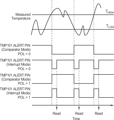 Figure 11. Output Transfer Function Diagrams
7.5.3.4 Fault Queue (F1, F0)
A fault condition occurs when the measured temperature exceeds the user-defined limits set in the THIGH and TLOW Registers. Additionally, the number of fault conditions required to generate an alert can be programmed using the Fault Queue. The Fault Queue is provided to prevent a false alert resulting from environmental noise. The Fault Queue requires consecutive fault measurements in order to trigger the alert function. If the temperature falls below TLOW before reaching the number of programmed consecutive faults limit, the count is reset to 0. Table 9 defines the number of measured faults that can be programmed to trigger an alert condition in the device.
Table 9. Fault Settings of the TMP100 and TMP101
| F1 | F0 | CONSECUTIVE FAULTS |
|---|---|---|
| 0 | 0 | 1 |
| 0 | 1 | 2 |
| 1 | 0 | 4 |
| 1 | 1 | 6 |
7.5.3.5 Converter Resolution (R1, R0)
The Converter Resolution bits control the resolution of the internal analog-to-digital converter (ADC), thus allowing the user to maximize efficiency by programming for higher resolution or faster conversion time. Table 10 identifies the Resolution bits and the relationship between resolution and conversion time.
Table 10. Resolution of the TMP100 and TMP101
| R1 | R0 | RESOLUTION | CONVERSION TIME (Typical) |
|---|---|---|---|
| 0 | 0 | 9 bits (0.5°C) | 40 ms |
| 0 | 1 | 10 bits (0.25°C) | 80 ms |
| 1 | 0 | 11 bits (0.125°C) | 160 ms |
| 1 | 1 | 12 bits (0.0625°C) | 320 ms |
7.5.3.6 OS/ALERT (OS)
The TMP100 and TMP101 devices feature a One-Shot Temperature Measurement Mode. When the device is in Shutdown Mode, writing 1 to the OS/ALERT bit starts a single temperature conversion. The device returns to the shutdown state at the completion of the single conversion. This feature is useful to reduce power consumption in the TMP100 and TMP101 when continuous temperature monitoring is not required.
Reading the OS/ALERT bit provides information about the Comparator Mode status. The state of the POL bit inverts the polarity of data returned from the OS/ALERT bit. For POL = 0, the OS/ALERT reads as 1 until the temperature equals or exceeds THIGH for the programmed number of consecutive faults, causing the OS/ALERT bit to read as 0. The OS/ALERT bit continues to read as 0 until the temperature falls below TLOW for the programmed number of consecutive faults when the OS/ALERT bit again reads as 1. The status of the TM bit does not affect the status of the OS/ALERT bit.
7.5.4 High- and Low-Limit Registers
In Comparator Mode (TM = 0), the ALERT pin of the TMP101 becomes active when the temperature equals or exceeds the value in THIGH and generates a consecutive number of faults according to fault bits F1 and F0. The ALERT pin remains active until the temperature falls below the indicated TLOW value for the same number of faults.
In Interrupt Mode (TM = 1) the ALERT pin becomes active when the temperature equals or exceeds THIGH for a consecutive number of fault conditions. The ALERT pin remains active until a read operation of any register occurs or the device successfully responds to the SMBus Alert Response Address. The ALERT pin is also cleared if the device is placed in Shutdown Mode. When the ALERT pin is cleared, it only becomes active again by the temperature falling below TLOW. When the temperature falls below TLOW, the ALERT pin becomes active and remains active until cleared by a read operation of any register or a successful response to the SMBus Alert Response Address. When the ALERT pin is cleared, the above cycle repeats with the ALERT pin becoming active when the temperature equals or exceeds THIGH. The ALERT pin can also be cleared by resetting the device with the General Call Reset command. This action also clears the state of the internal registers in the device, returning the device to Comparator Mode (TM = 0).
Both operational modes are represented in Figure 11. Table 11, Table 12, Table 13, and Table 14 describe the format for the THIGH and TLOW registers. Power-up reset values for THIGH and TLOW are: THIGH = 80°C and TLOW = 75°C. The format of the data for THIGH and TLOW is the same as for the Temperature Register.
Table 11. Byte 1 of the THIGH Register
| D7 | D6 | D5 | D4 | D3 | D2 | D1 | D0 |
|---|---|---|---|---|---|---|---|
| H11 | H10 | H9 | H8 | H7 | H6 | H5 | H4 |
Table 12. Byte 2 of the THIGH Register
| D7 | D6 | D5 | D4 | D3 | D2 | D1 | D0 |
|---|---|---|---|---|---|---|---|
| H3 | H2 | H1 | H0 | 0 | 0 | 0 | 0 |
Table 13. Byte 1 of the TLOW Register
| D7 | D6 | D5 | D4 | D3 | D2 | D1 | D0 |
|---|---|---|---|---|---|---|---|
| L11 | L10 | L9 | L8 | L7 | L6 | L5 | L4 |
Table 14. Byte 2 of the TLOW Register
| D7 | D6 | D5 | D4 | D3 | D2 | D1 | D0 |
|---|---|---|---|---|---|---|---|
| L3 | L2 | L1 | L0 | 0 | 0 | 0 | 0 |
All 12 bits for the Temperature, THIGH, and TLOW registers are used in the comparisons for the ALERT function for all converter resolutions. The three LSBs in THIGH and TLOW can affect the ALERT output even if the converter is configured for 9-bit resolution.