SBOS397H August   2007  – December 2018 TMP102

PRODUCTION DATA.  

  1. Features
  2. Applications
    1.     Simplified Schematic
  3. Description
    1.     Block Diagram
  4. Revision History
  5. Pin Configuration and Functions
    1.     Pin Functions
  6. Specifications
    1. 6.1 Absolute Maximum Ratings
    2. 6.2 Handling Ratings
    3. 6.3 Recommended Operating Conditions
    4. 6.4 Thermal Information
    5. 6.5 Electrical Characteristics
    6. 6.6 Timing Requirements
    7. 6.7 Typical Characteristics
  7. Detailed Description
    1. 7.1 Overview
    2. 7.2 Functional Block Diagram
    3. 7.3 Feature Description
      1. 7.3.1  Digital Temperature Output
        1. Table 2. 12-Bit Temperature Data Format
      2. 7.3.2  Serial Interface
      3. 7.3.3  Bus Overview
      4. 7.3.4  Serial Bus Address
      5. 7.3.5  Writing and Reading Operation
      6. 7.3.6  Slave Mode Operations
        1. 7.3.6.1 Slave Receiver Mode
        2. 7.3.6.2 Slave Transmitter Mode
      7. 7.3.7  SMBus Alert Function
      8. 7.3.8  General Call
      9. 7.3.9  High-Speed (HS) Mode
      10. 7.3.10 Timeout Function
      11. 7.3.11 Timing Diagrams
    4. 7.4 Device Functional Modes
      1. 7.4.1 Continuos-Conversion Mode
      2. 7.4.2 Extended Mode (EM)
      3. 7.4.3 Shutdown Mode (SD)
      4. 7.4.4 One-Shot/Conversion Ready (OS)
      5. 7.4.5 Thermostat Mode (TM)
        1. 7.4.5.1 Comparator Mode (TM = 0)
        2. 7.4.5.2 Interrupt Mode (TM = 1)
    5. 7.5 Programming
      1. 7.5.1 Pointer Register
        1. Table 7. Pointer Addresses
      2. 7.5.2 Temperature Register
        1. Table 8. Byte 1 of Temperature Register
        2. Table 9. Byte 2 of Temperature Register
      3. 7.5.3 Configuration Register
        1. Table 10. Byte 1 of Configuration and Power-Up or Reset Format
        2. Table 11. Byte 2 of Configuration and Power-Up or Reset Format
        3. 7.5.3.1   Shutdown Mode (SD)
        4. 7.5.3.2   Thermostat Mode (TM)
        5. 7.5.3.3   Polarity (POL)
        6. 7.5.3.4   Fault Queue (F1/F0)
        7. 7.5.3.5   Converter Resolution (R1/R0)
        8. 7.5.3.6   One-Shot (OS)
        9. 7.5.3.7   EM Bit
        10. 7.5.3.8   Alert (AL Bit)
        11. 7.5.3.9   Conversion Rate (CR)
      4. 7.5.4 High- and Low-Limit Registers
        1. Table 13. Byte 1 Temperature Register HIGH
        2. Table 14. Byte 2 Temperature Register HIGH
        3. Table 15. Byte 1 Temperature Register LOW
        4. Table 16. Byte 2 Temperature Register LOW
  8. Application and Implementation
    1. 8.1 Application Information
    2. 8.2 Typical Application
      1. 8.2.1 Design Requirements
      2. 8.2.2 Detailed Design Procedure
      3. 8.2.3 Application Curve
  9. Power Supply Recommendations
  10. 10Layout
    1. 10.1 Layout Guidelines
    2. 10.2 Layout Example
  11. 11Device and Documentation Support
    1. 11.1 Documentation Support
      1. 11.1.1 Related Documentation
    2. 11.2 Receiving Notification of Documentation Updates
    3. 11.3 Community Resources
    4. 11.4 Trademarks
    5. 11.5 Electrostatic Discharge Caution
    6. 11.6 Glossary
  12. 12Mechanical, Packaging, and Orderable Information

Package Options

Mechanical Data (Package|Pins)
Thermal pad, mechanical data (Package|Pins)
Orderable Information

Application Curve

Figure 16 shows the step response of the TMP102 device to a submersion in an oil bath of 100ºC from room temperature (27ºC). The time-constant, or the time for the output to reach 63% of the input step, is 0.8 s. The time-constant result depends on the printed circuit board (PCB) that the TMP102 device is mounted. For this test, the TMP102 device was soldered to a two-layer PCB that measured 0.375 inch × 0.437 inch.

space
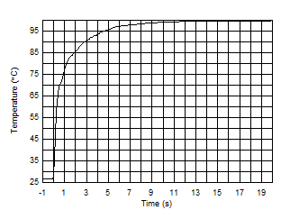
TMP102 AppGraph_SLOS887_TMP112-Q1.gifFigure 16. Temperature Step Response