SBOS545D February 2011 – December 2018 TMP103
PRODUCTION DATA.
- 1 Features
- 2 Applications
- 3 Description
- 4 Revision History
- 5 Pin Configuration and Functions
- 6 Specifications
-
7 Detailed Description
- 7.1 Overview
- 7.2 Functional Block Diagram
- 7.3 Feature Description
- 7.4 Device Functional Modes
- 7.5
Programming
- 7.5.1 Temperature Watchdog Function
- 7.5.2 Conversion Rate
- 7.5.3 Shutdown Mode (M1 = 0, M0 = 0)
- 7.5.4 One-Shot (M1 = 0, M0 = 1)
- 7.5.5 Continuous Conversion Mode (M1 = 1)
- 7.5.6 Bus Overview
- 7.5.7 Serial Interface
- 7.5.8 Serial Bus Address
- 7.5.9 Writing and Reading Operation
- 7.5.10 Slave Mode Operations
- 7.5.11 General Call
- 7.5.12 High-Speed (Hs) Mode
- 7.5.13 Timeout Function
- 7.5.14 Multiple Device Access
- 7.5.15 NOISE
- 7.6 Register Maps
- 8 Application and Implementation
- 9 Power Supply Recommendations
- 10Layout
- 11Device and Documentation Support
- 12Mechanical, Packaging, and Orderable Information
Package Options
Refer to the PDF data sheet for device specific package drawings
Mechanical Data (Package|Pins)
- YFF|4
Thermal pad, mechanical data (Package|Pins)
Orderable Information
6.6 Timing Requirements
See (1)| FAST MODE | HIGH-SPEED MODE | UNIT | ||||
|---|---|---|---|---|---|---|
| MIN | MAX | MIN | MAX | |||
| f(SCL) | SCL operating frequency, VS > 1.7 V | 0.001 | 0.4 | 0.001 | 3.4 | MHz |
| f(SCL) | SCL operating frequency, VS < 1.7 V | 0.001 | 0.4 | 0.001 | 2.75 | MHz |
| t(BUF) | Bus free time between STOP and START condition | 600 | 160 | ns | ||
| t(HDSTA) | Hold time after repeated START condition.
After this period, the first clock is generated. |
100 | 100 | ns | ||
| t(SUSTA) | Repeated START condition setup time | 100 | 100 | ns | ||
| t(SUSTO) | STOP condition setup Time | 100 | 100 | ns | ||
| t(HDDAT) | Data hold time | 20 | 400 | 10 | 125 | ns |
| t(SUDAT) | Data setup time | 100 | 10 | ns | ||
| t(LOW) | SCL clock low period, VS > 1.7 V | 1300 | 160 | ns | ||
| t(LOW) | SCL clock low period, VS < 1.7 V | 1300 | 200 | ns | ||
| t(HIGH) | SCL clock high period | 600 | 60 | ns | ||
| tF | Clock/data fall time | 300 | ns | |||
| tR | Clock/data rise time | 300 | 160 | ns | ||
| tR | Clock/data rise time for SCLK ≤ 100 kHz | 1000 | ns | |||
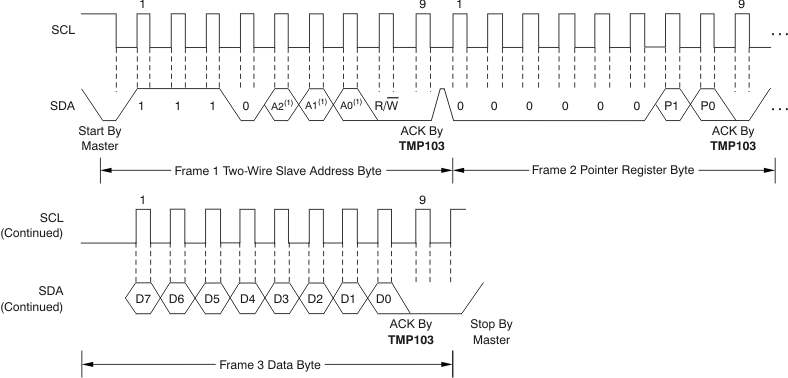
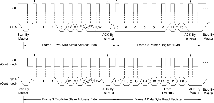
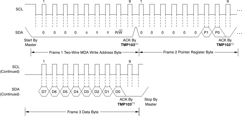
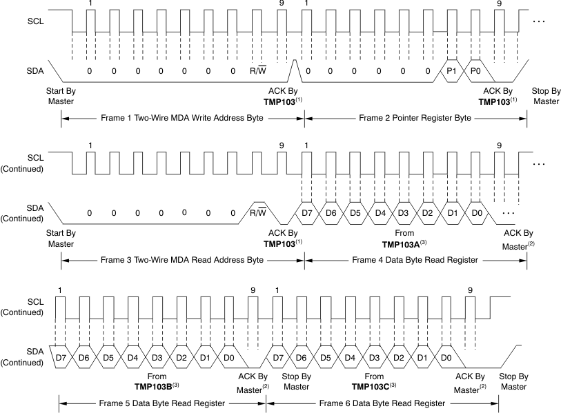
The TMP103 is two-wire and SMBus compatible. Figure 1 to Figure 5 describe the various operations on the TMP103. Parameters for Figure 1 are defined in Timing Requirements. Bus definitions are:
Bus Idle: Both SDA and SCL lines remain high.
Start Data Transfer: A change in the state of the SDA line, from high to low, while the SCL line is high, defines a START condition. Each data transfer is initiated with a START condition.
Stop Data Transfer: A change in the state of the SDA line from low to high while the SCL line is high defines a STOP condition. Each data transfer is terminated with a repeated START or STOP condition.
Data Transfer: The number of data bytes transferred between a START and a STOP condition is not limited and is determined by the master device.
Acknowledge: Each receiving device, when addressed, is obliged to generate an Acknowledge bit. A device that acknowledges must pull down the SDA line during the Acknowledge clock pulse in such a way that the SDA line is stable low during the high period of the Acknowledge clock pulse. Setup and hold times must be taken into account. On a master receive, the termination of the data transfer can be signaled by the master generating a Not-Acknowledge (1) on the last byte transmitted by the slave.


