SBOS583B December 2011 – December 2016 TMP709
PRODUCTION DATA.
- 1 Features
- 2 Applications
- 3 Description
- 4 Revision History
- 5 Pin Configuration and Functions
- 6 Specifications
- 7 Detailed Description
- 8 Applications and Implementation
- 9 Power Supply Recommendations
- 10Layout
- 11Device and Documentation Support
- 12Mechanical, Packaging, and Orderable Information
Package Options
Mechanical Data (Package|Pins)
- DBV|5
Thermal pad, mechanical data (Package|Pins)
Orderable Information
10 Layout
10.1 Layout Guidelines
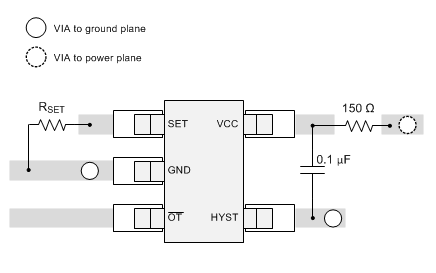
The TMP709 is extremely simple to lay out. Figure 7 shows the recommended board layout.
10.2 Layout Example
 Figure 7. Recommended Layout
10.3 Thermal Considerations
The TMP709 quiescent current is typically 40 μA. The device dissipates negligible power when the output drives a high-impedance load. Thus, the die temperature is the same as the package temperature. In order to maintain accurate temperature monitoring, provide a good thermal contact between the TMP709 package and the device being monitored. The rise in die temperature as a result of self-heating is given by Equation 2:
Equation 2. ΔTJ = PDISS × θJA
where
- PDISS = power dissipated by the device.
- θJA = package thermal resistance. Typical thermal resistance for SOT-23 package is 217.9°C/W.
To limit the effects of self-heating, keep the output current at a minimum level.