SPRS737C August 2011 – April 2014 TMS320C5532 , TMS320C5533 , TMS320C5534 , TMS320C5535
PRODUCTION DATA.
- 1Device Overview
- 2Revision History
- 3Device Comparison
-
4Terminal Configuration and Functions
- 4.1 Pin Diagram
- 4.2
Signal Descriptions
- 4.2.1 Oscillator and PLL
- 4.2.2 Real-Time Clock (RTC)
- 4.2.3 RESET, Interrupts, and JTAG
- 4.2.4 Inter-Integrated Circuit (I2C)
- 4.2.5 Inter-IC Sound (I2S)
- 4.2.6 Serial Peripheral Interface (SPI)
- 4.2.7 Universal Asynchronous Receiver/Transmitter (UART)
- 4.2.8 Universal Serial Bus (USB) 2.0
- 4.2.9 LCD Bridge
- 4.2.10 Secure Digital (SD)
- 4.2.11 Successive Approximation (SAR) Analog-to-Digital Converter (ADC)
- 4.2.12 General-Purpose Input/Output (GPIO)
- 4.2.13 Regulators and Power Management
- 4.2.14 Reserved and No Connects
- 4.2.15 Supply Voltage
- 4.2.16 Ground
- 4.3 Pin Multiplexing
-
5Specifications
- 5.1 Absolute Maximum Ratings
- 5.2 Recommended Operating Conditions
- 5.3 Electrical Characteristics
- 5.4 Handling Ratings
- 5.5 Thermal Characteristics
- 5.6 Power-On Hours
- 5.7
Timing and Switching Characteristics
- 5.7.1 Parameter Information
- 5.7.2
Power Supplies
- 5.7.2.1 Power Considerations for C5535 and C5534
- 5.7.2.2 Power Considerations for C5533
- 5.7.2.3 Power Considerations for C5532
- 5.7.2.4 Power-Supply Sequencing
- 5.7.2.5 Digital I/O Behavior When Core Power (CVDD) is Down
- 5.7.2.6 Power-Supply Design Considerations
- 5.7.2.7 Power-Supply Decoupling
- 5.7.2.8 LDO Input Decoupling
- 5.7.2.9 LDO Output Decoupling
- 5.7.3
Reset
- 5.7.3.1 Power-On Reset (POR) Circuits
- 5.7.3.2 Pin Behavior at Reset
- 5.7.3.3 Reset Electrical Data and Timing
- 5.7.3.4 Configurations at Reset
- 5.7.3.5
Configurations After Reset
- 5.7.3.5.1 External Bus Selection Register (EBSR)
- 5.7.3.5.2 LDO Control Register [7004h]
- 5.7.3.5.3 USB System Control Registers (USBSCR) [1C32h]
- 5.7.3.5.4 Peripheral Clock Gating Control Registers (PCGCR1 and PCGCR2) [1C02h and 1C03h]
- 5.7.3.5.5 Pullup and Pulldown Inhibit Registers (PDINHIBR1, 2, and 3) [1C17h, 1C18h, and 1C19h]
- 5.7.3.5.6 Output Slew Rate Control Register (OSRCR) [1C16h]
- 5.7.4
Clock Specifications
- 5.7.4.1 Recommended Clock and Control Signal Transition Behavior
- 5.7.4.2 Clock Considerations
- 5.7.4.3 PLLs
- 5.7.4.4 Input and Output Clocks Electrical Data and Timing
- 5.7.4.5 Wake-up Events, Interrupts, and XF
- 5.7.5 Direct Memory Access (DMA) Controller
- 5.7.6 General-Purpose Input/Output
- 5.7.7 General-Purpose Timers
- 5.7.8 Inter-Integrated Circuit (I2C)
- 5.7.9 Inter-IC Sound (I2S)
- 5.7.10 Liquid Crystal Display Controller (LCDC) — C5535 Only
- 5.7.11 Real-Time Clock (RTC)
- 5.7.12 SAR ADC (10-Bit) — C5535 Only
- 5.7.13 Secure Digital (SD)
- 5.7.14 Serial Port Interface (SPI)
- 5.7.15 Universal Asynchronous Receiver/Transmitter (UART)
- 5.7.16 Universal Serial Bus (USB) 2.0 Controller — Does Not Apply to C5532
- 5.7.17 Emulation and Debug
- 5.7.18 IEEE 1149.1 JTAG
-
6Detailed Description
- 6.1 CPU
- 6.2
Memory
- 6.2.1 Internal Memory
- 6.2.2 Memory Map
- 6.2.3
Register Map
- 6.2.3.1 General-Purpose Input/Output Peripheral Register Descriptions
- 6.2.3.2 I2C Peripheral Register Descriptions
- 6.2.3.3 I2S Peripheral Register Descriptions
- 6.2.3.4 LCDC Peripheral Register Descriptions
- 6.2.3.5 RTC Peripheral Register Descriptions
- 6.2.3.6 SAR ADC Peripheral Register Descriptions
- 6.2.3.7 SD Peripheral Register Descriptions
- 6.2.3.8 SPI Peripheral Register Descriptions
- 6.2.3.9 System Registers
- 6.2.3.10 Timers Peripheral Register Descriptions
- 6.2.3.11 UART Peripheral Register Descriptions
- 6.2.3.12 USB2.0 Peripheral Register Descriptions
- 6.3 Identification
- 6.4 Boot Modes
- 7Device and Documentation Support
- 8Mechanical Packaging and Orderable Information
Package Options
Refer to the PDF data sheet for device specific package drawings
Mechanical Data (Package|Pins)
- ZAY|144
Thermal pad, mechanical data (Package|Pins)
Orderable Information
4 Terminal Configuration and Functions
4.1 Pin Diagram
The following figures show the bottom view of the package pin assignments.
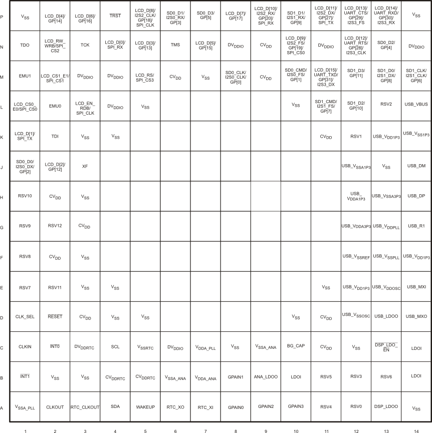 Figure 4-1 C5535 Pin Diagram
 Figure 4-2 C5534 Pin Diagram
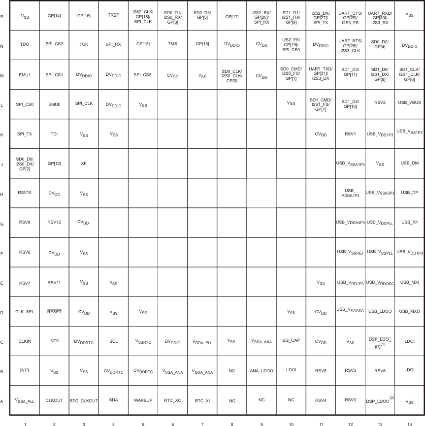
4.2 Signal Descriptions
The signal descriptions tables (Table 4-1 through Table 4-18) identify the external signal names, the associated pin (ball) numbers along with the mechanical package designator, the pin type, whether the pin has any internal pullup or pulldown resistors or bus-holders, and a functional pin description. For more information on pin multiplexing, see Section 4.3, Pin Multiplexing.
For proper device operation, external pullup and pulldown resistors may be required on some pins. Section 5.7.17.1.1, Pullup and Pulldown Resistors discusses situations where external pullup and pulldown resistors are required.
4.2.1 Oscillator and PLL
Table 4-1 Oscillator and PLL Signal Descriptions
| SIGNAL | TYPE (1)(4) |
OTHER(2)(3) | DESCRIPTION | ||||
|---|---|---|---|---|---|---|---|
| NAME | NO. | ||||||
| CLKOUT | A2 | O/Z | – DVDDIO BH |
DSP clock output signal. For debug purposes only, the CLKOUT pin can be used to tap different clocks within the system clock generator. The SRC bits in the CLKOUT Control Source Register (CCSSR) can be used to specify the CLKOUT pin source. Additionally, the slew rate of the CLKOUT pin can be controlled by the Output Slew Rate Control Register (OSRCR) [1C16h]. The CLKOUT pin is enabled and disabled through the CLKOFF bit in the CPU ST3_55 register. When disabled, the CLKOUT pin is placed in high-impedance (Hi-Z). At reset the CLKOUT pin is enabled until the beginning of the boot sequence, when the on-chip bootloader sets CLKOFF = 1 and the CLKOUT pin is disabled (Hi-Z). For more information on the ST3_55 register, see the TMS320C55x 3.0 CPU Reference Guide (literature number: SWPU073). Note: This pin may consume static power if configured as Hi-Z and not externally pulled low or high. Prevent current drain by externally terminating the pin. |
|||
| CLKIN | C1 | I | – DVDDIO BH |
Input clock. This signal is used to input an external clock when the 32-kHz on-chip oscillator is not used as the DSP clock (pin CLK_SEL = 1). For boot purposes, the CLKIN frequency is assumed to be either 11.2896, 12, or 12.288 MHz. The CLK_SEL pin (D1) selects between the 32-kHz crystal clock or CLKIN. When the CLK_SEL pin is low, this pin must be tied to ground (VSS). When CLK_SEL is high, this pin must be driven by an external clock source. If CLK_SEL is high, this pin is used as the reference clock for the clock generator. During bootup, the bootloader bypasses the PLL and assumes the CLKIN frequency is one of the following frequencies: 11.2896-, 12-, or 12.288-MHz. In addition, the bootloader sets the SPI clock rate at 500 kHz and the I2C clock rate at 400 kHz . |
|||
| CLK_SEL | D1 | I | – DVDDIO BH |
Clock input select. This pin selects between the 32-kHz crystal clock or CLKIN. 0 = 32-kHz on-chip oscillator drives the RTC timer and the system clock generator while CLKIN is ignored. 1 = CLKIN drives the system clock generator and the 32-kHz on-chip oscillator drives only the RTC timer. This pin is not allowed to change during device operation; it must be tied high or low at the board. |
|||
| VDDA_PLL | C7 | PWR | see Section 5.2, ROC | 1.3-V Analog PLL power supply for the system clock generator (PLLOUT ≤ 120 MHz). This signal can be powered from the ANA_LDOO pin. |
|||
| VSSA_PLL | A1 | GND | see Section 5.2, ROC | Analog PLL ground for the system clock generator. | |||
4.2.2 Real-Time Clock (RTC)
Table 4-2 RTC Signal Descriptions
| SIGNAL | TYPE (1)(4) |
OTHER(2)(3) | DESCRIPTION | ||||
|---|---|---|---|---|---|---|---|
| NAME | NO. | ||||||
| RTC_XO | A6 | I/O/Z | – CVDDRTC DVDDRTC |
Real-time clock oscillator output. This pin operates at the RTC core voltage, CVDDRTC, and supports a 32.768-kHz crystal. If the RTC oscillator is not used, it can be disabled by connecting RTC_XI to CVDDRTC and RTC_XO to ground (VSS). A voltage must still be applied to CVDDRTC by an external power source (see Section 5.2, Recommended Operating Conditions). None of the on-chip LDOs can be used to power CVDDRTC. Note: When RTC oscillator is disabled, the RTC registers (I/O address range 1900h – 197Fh) are not accessible. |
|||
| RTC_XI | A7 | I | – CVDDRTC DVDDRTC |
Real-time clock oscillator input. If the RTC oscillator is not used, it can be disabled by connecting RTC_XI to CVDDRTC and RTC_XO to ground (VSS). A voltage must still be applied to CVDDRTC by an external power source (see Section 5.2, Recommended Operating Conditions). None of the on-chip LDOs can be used to power CVDDRTC. Note: When RTC oscillator is disabled, the RTC registers (I/O address range 1900h – 197Fh) are not accessible. |
|||
| RTC_CLKOUT | A3 | O/Z | – DVDDRTC |
Real-time clock output pin. This pin operates at DVDDRTC voltage. The RTC_CLKOUT pin is enabled and disabled through the RTCCLKOUTEN bit in the RTC Power Management Register (RTCPMGT). At reset, the RTC_CLKOUT pin is disabled (high-impedance [Hi-Z]). | |||
| WAKEUP | A5 | I/O/Z | – DVDDRTC |
The pin is used to WAKEUP the core from idle condition. This pin defaults to an input at CVDDRTC powerup, but can also be configured as an active-low open-drain output signal to wakeup an external device from an RTC alarm. | |||
4.2.3 RESET, Interrupts, and JTAG
Table 4-3 RESET, Interrupts, and JTAG Signal Descriptions
| SIGNAL | TYPE (1)(4) |
OTHER(2)(3) | DESCRIPTION | ||||
|---|---|---|---|---|---|---|---|
| NAME | NO. | ||||||
| RESET | |||||||
| XF | J3 | O/Z | – DVDDIO BH |
External Flag Output. XF is used for signaling other processors in multiprocessor configurations or XF can be used as a fast general-purpose output pin. XF is set high by the BSET XF instruction and XF is set low by the BCLR XF instruction or by writing to bit 13 of the ST1_55 register. For more information on the ST1_55 register, see the TMS320C55x 3.0 CPU Reference Guide (literature number: SWPU073). For XF pin behavior at reset, see Section 5.7.3.2, Pin Behavior at Reset. Note: This pin may consume static power if configured as Hi-Z and not externally pulled low or high. Prevent current drain by externally terminating the pin. XF pin is ONLY in the Hi-Z state when doing boundary scan. Therefore, external termination is probably not required for most applications. |
|||
| RESET | D2 | I | IPU DVDDIO BH |
Device reset. RESET causes the DSP to terminate execution and loads the program counter with the contents of the reset vector. When RESET is brought to a high level, the reset vector in ROM at FFFF00h forces the program execution to branch to the location of the on-chip ROM bootloader. RESET affects the various registers and status bits. The IPU resistor on this pin can be enabled or disabled via the PDINHIBR2 register but will be forced ON when RESET is asserted. |
|||
| JTAG | |||||||
| [For more detailed information on emulation header design guidelines, see the XDS560 Emulator Technical Reference (literature number: SPRU589).] | |||||||
| TMS | N6 | I | IPU DVDDIO BH |
IEEE standard 1149.1 test mode select. This serial control input is clocked into the TAP controller on the rising edge of TCK. If the emulation header is located greater than 6 inches from the device, TMS must be buffered. In this case, the input buffer for TMS needs a pullup resistor connected to DVDDIO to hold the signal at a known value when the emulator is not connected. A resistor value of 4.7 kΩ or greater is suggested. For board design guidelines related to the emulation header, see the XDS560 Emulator Technical Reference (literature number: SPRU589). The IPU resistor on this pin can be enabled or disabled via the PDINHIBR2 register. |
|||
| TDO | N1 | O/Z | – DVDDIO BH |
IEEE standard 1149.1 test data output. The contents of the selected register (instruction or data) are shifted out of TDO on the falling edge of TCK. TDO is in the high-impedance (Hi-Z) state except when the scanning of data is in progress. For board design guidelines related to the emulation header, see the XDS560 Emulator Technical Reference (literature number: SPRU589). If the emulation header is located greater than 6 inches from the device, TDO must be buffered. Note: This pin may consume static power if configured as Hi-Z and not externally pulled low or high. Prevent current drain by externally terminating the pin. TDO pin will be in Hi-Z whenever not doing emulation and boundary scan, so an external pullup is highly recommended. |
|||
| TDI | K2 | I | IPU DVDDIO BH |
IEEE standard 1149.1 test data input. TDI is clocked into the selected register (instruction or data) on a rising edge of TCK. If the emulation header is located greater than 6 inches from the device, TDI must be buffered. In this case, the input buffer for TDI needs a pullup resistor connected to DVDDIO to hold this signal at a known value when the emulator is not connected. A resistor value of 4.7 kΩ or greater is suggested. The IPU resistor on this pin can be enabled or disabled via the PDINHIBR2 register. |
|||
| TCK | N3 | I | IPU DVDDIO BH |
IEEE standard 1149.1 test clock. TCK is normally a free-running clock signal with a 50% duty cycle. The changes on input signals TMS and TDI are clocked into the TAP controller, instruction register, or selected test data register on the rising edge of TCK. Changes at the TAP output signal (TDO) occur on the falling edge of TCK. If the emulation header is located greater than 6 inches from the device, TCK must be buffered. For board design guidelines related to the emulation header, see the XDS560 Emulator Technical Reference (literature number: SPRU589). The IPU resistor on this pin can be enabled or disabled via the PDINHIBR2 register. |
|||
| TRST | P4 | I | IPD DVDDIO BH |
IEEE standard 1149.1 reset signal for test and emulation logic. TRST, when high, allows the IEEE standard 1149.1 scan and emulation logic to take control of the operations of the device. If TRST is not connected or is driven low, the device operates in its functional mode, and the IEEE standard 1149.1 signals are ignored. The device will not operate properly if this reset pin is never asserted low. For board design guidelines related to the emulation header, see the XDS560 Emulator Technical Reference (literature number: SPRU589). It is recommended that an external pulldown resistor be used in addition to the IPD -- especially if there is a long trace to an emulation header. |
|||
| EMU1 | M1 | I/O/Z | IPU DVDDIO BH |
Emulator 1 pin. EMU1 is used as an interrupt to or from the emulator system and is defined as input/output by way of the emulation logic. For board design guidelines related to the emulation header, see the XDS560 Emulator Technical Reference (literature number: SPRU589). An external pullup to DVDDIO is required to provide a signal rise time of less than 10 μsec. A 4.7-kΩ resistor is suggested for most applications. For board design guidelines related to the emulation header, see the XDS560 Emulator Technical Reference (literature number: SPRU589). The IPU resistor on this pin can be enabled or disabled via the PDINHIBR2 register. |
|||
| EMU0 | L2 | I/O/Z | IPU DVDDIO BH |
Emulator 0 pin. When TRST is driven low and then high, the state of the EMU0 pin is latched and used to connect the JTAG pins (TCK, TMS, TDI, TDO) to either the IEEE1149.1 Boundary-Scan TAP (when the latched value of EMU0 = 0) or to the DSP Emulation TAP (when the latched value of EMU0 = 1). Once TRST is high, EMU0 is used as an interrupt to or from the emulator system and is defined as input/output by way of the emulation logic. An external pullup to DVDDIO is required to provide a signal rise time of less than 10 μsec. A 4.7-kΩ resistor is suggested for most applications. For board design guidelines related to the emulation header, see the XDS560 Emulator Technical Reference (literature number: SPRU589). The IPU resistor on this pin can be enabled or disabled via the PDINHIBR2 register. |
|||
| EXTERNAL INTERRUPTS | |||||||
| INT1 | B1 | I | IPU DVDDIO BH |
External interrupt inputs (INT1 and INT0). These pins are maskable via their specific Interrupt Mask Register (IMR1, IMR0) and the interrupt mode bit. The pins can be polled and reset by their specific Interrupt Flag Register (IFR1, IFR0). The IPU resistor on these pins can be enabled or disabled via the PDINHIBR2 register. |
|||
| INT0 | C2 | I | IPU DVDDIO BH |
||||
4.2.4 Inter-Integrated Circuit (I2C)
Table 4-4 I2C Signal Descriptions
| SIGNAL | TYPE (1)(4) |
OTHER(2)(3) | DESCRIPTION | ||||
|---|---|---|---|---|---|---|---|
| NAME | NO. | ||||||
| I2C | |||||||
| SCL | C4 | I/O/Z | DVDDIO BH |
This pin is the I2C clock output. Per the I2C standard, an external pullup is required on this pin. | |||
| SDA | A4 | I/O/Z | DVDDIO BH |
This pin is the I2C bidirectional data signal. Per the I2C standard, an external pullup is required on this pin. | |||
4.2.5 Inter-IC Sound (I2S)
Table 4-5 I2S0 – I2S3 Signal Descriptions
| SIGNAL | TYPE (2)(5) |
OTHER(3)(4) | DESCRIPTION(1) | ||||
|---|---|---|---|---|---|---|---|
| NAME(1) | NO. | ||||||
| Interface 0 (I2S0) | |||||||
| SD0_D0/ I2S0_DX/ GP[2] |
J1 | I/O/Z | IPD DVDDIO BH |
This pin is multiplexed between SD0, I2S0, and GPIO. For I2S, it is I2S0 transmit data output I2S0_DX. Mux control via the SP0MODE bits in the EBSR. The IPD resistor on this pin can be enabled or disabled via the PDINHIBR1 register. |
|||
| SD0_CLK/ I2S0_CLK/ GP[0] |
M8 | I/O/Z | IPD DVDDIO BH |
This pin is multiplexed between SD0, I2S0, and GPIO. For I2S, it is I2S0 clock input/output I2S0_CLK. Mux control via the SP0MODE bits in the EBSR. The IPD resistor on this pin can be enabled or disabled via the PDINHIBR1 register. |
|||
| SD0_D1/ I2S0_RX/ GP[3] |
P6 | I/O/Z | IPD DVDDIO BH |
This pin is multiplexed between SD0, I2S0, and GPIO. For I2S, it is I2S0 receive data input I2S0_RX. Mux control via the SP0MODE bits in the EBSR. The IPD resistor on this pin can be enabled or disabled via the PDINHIBR1 register. |
|||
| SD0_CMD/ I2S0_FS/ GP[1] |
M10 | I/O/Z | IPD DVDDIO BH |
This pin is multiplexed between SD0, I2S0, and GPIO. For I2S, it is I2S0 frame synchronization input/output I2S0_FS. Mux control via the SP0MODE bits in the EBSR. The IPD resistor on this pin can be enabled or disabled via the PDINHIBR1 register. |
|||
| Interface 1 (I2S1) | |||||||
| SD1_D0/ I2S1_DX/ GP[8] |
M13 | I/O/Z | IPD DVDDIO BH |
This pin is multiplexed between SD1, I2S1, and GPIO. For I2S, it is I2S1 transmit data output I2S1_DX. Mux control via the SP1MODE bits in the EBSR. The IPD resistor on this pin can be enabled or disabled via the PDINHIBR1 register. |
|||
| SD1_CLK/ I2S1_CLK/ GP[6] |
M14 | I/O/Z | IPD DVDDIO BH |
This pin is multiplexed between SD1, I2S1, and GPIO. For I2S, it is I2S1 clock input/output I2S1_CLK. Mux control via the SP1MODE bits in the EBSR. The IPD resistor on this pin can be enabled or disabled via the PDINHIBR1 register. |
|||
| SD1_D1/ I2S1_RX/ GP[9] |
P10 | I/O/Z | IPD DVDDIO BH |
This pin is multiplexed between SD1, I2S1, and GPIO. For I2S, it is I2S1 receive data input I2S1_RX. Mux control via the SP1MODE bits in the EBSR. The IPD resistor on this pin can be enabled or disabled via the PDINHIBR1 register. |
|||
| SD1_CMD/ I2S1_FS/ GP[7] |
L11 | I/O/Z | IPD DVDDIO BH |
This pin is multiplexed between SD1, I2S2, and GPIO. For I2S, it is I2S1 frame synchronization input/output I2S1_FS. Mux control via the SP1MODE bits in the EBSR. The IPD resistor on this pin can be enabled or disabled via the PDINHIBR1 register. |
|||
| Interface 2 (I2S2) | |||||||
| LCD_D[11]/ I2S2_DX/ GP[27]/ SPI_TX |
P11 | I/O/Z | IPD DVDDIO BH |
This pin is multiplexed between LCD Bridge, I2S2, GPIO, and SPI. For I2S, it is I2S2 transmit data output I2S2_DX. Mux control via the PPMODE bits in the EBSR. The IPD resistor on this pin can be enabled or disabled via the PDINHIBR3 register. |
|||
| LCD_D[8]/ I2S2_CLK/ GP[18]/ SPI_CLK |
P5 | I/O/Z | IPD DVDDIO BH |
This pin is multiplexed between LCD Bridge, I2S2, GPIO, and SPI. For I2S, it is I2S2 clock input/output I2S2_CLK. Mux control via the PPMODE bits in the EBSR. The IPD resistor on this pin can be enabled or disabled via the PDINHIBR3 register. |
|||
| LCD_D[10]/ I2S2_RX/ GP[20]/ SPI_RX |
P9 | I/O/Z | IPD DVDDIO BH |
This pin is multiplexed between LCD Bridge, I2S2, GPIO, and SPI. For I2S, it is I2S2 receive data input I2S2_RX. Mux control via the PPMODE bits in the EBSR. The IPD resistor on this pin can be enabled or disabled via the PDINHIBR3 register. |
|||
| LCD_D[9]/ I2S2_FS/ GP[19]/ SPI_CS0 |
N10 | I/O/Z | IPD DVDDIO BH |
This pin is multiplexed between LCD Bridge, I2S2 and GPIO. For I2S, it is I2S2 frame synchronization input/output I2S2_FS. Mux control via the PPMODE bits in the EBSR. The IPD resistor on this pin can be enabled or disabled via the PDINHIBR3 register. |
|||
| Interface 3 (I2S3) | |||||||
| LCD_D[15]/ UART_TXD/ GP[31]/ I2S3_DX |
M11 | I/O/Z | IPD DVDDIO BH |
This pin is multiplexed between LCD Bridge, UART, GPIO, and I2S3. For I2S, it is I2S3 transmit data output I2S3_DX. Mux control via the PPMODE bits in the EBSR. The IPD resistor on this pin can be enabled or disabled via the PDINHIBR3 register. |
|||
| LCD_D[12]/ UART_RTS/ GP[28]/ I2S3_CLK |
N12 | I/O/Z | IPD DVDDIO BH |
This pin is multiplexed between LCD Bridge, UART, GPIO, and I2S3. For I2S, it is I2S3 clock input/output I2S3_CLK. Mux control via the PPMODE bits in the EBSR. The IPD resistor on this pin can be enabled or disabled via the PDINHIBR3 register. |
|||
| LCD_D[14]/ UART_RXD/ GP[30]/ I2S3_RX |
P13 | I/O/Z | IPD DVDDIO BH |
This pin is multiplexed between LCD Bridge, UART, GPIO, and I2S3. For I2S, it is I2S3 receive data input I2S3_RX. Mux control via the PPMODE bits in the EBSR. The IPD resistor on this pin can be enabled or disabled via the PDINHIBR3 register. |
|||
| LCD_D[13]/ UART_CTS/ GP[29]/ I2S3_FS |
P12 | I/O/Z | IPD DVDDIO BH |
This pin is multiplexed between LCD Bridge, UART, GPIO, and I2S3. For I2S, it is I2S3 frame synchronization input/output I2S3_FS. Mux control via the PPMODE bits in the EBSR. The IPD resistor on this pin can be enabled or disabled via the PDINHIBR3 register. |
|||
4.2.6 Serial Peripheral Interface (SPI)
Table 4-6 SPI Signal Descriptions
| SIGNAL | TYPE (2)(5) |
OTHER(3)(4) | DESCRIPTION(1) | ||||
|---|---|---|---|---|---|---|---|
| NAME(1) | NO. | ||||||
| Serial Port Interface (SPI) | |||||||
| LCD_CS0_E0/ SPI_CS0 |
L1 | I/O/Z | DVDDIO BH |
This pin is multiplexed between LCD Bridge and SPI. Mux control via the PPMODE bits in the EBSR. For SPI, this pin is SPI chip select SPI_CS0. |
|||
| LCD_D[9]/ I2S2_FS/ GP[19]/ SPI_CS0 |
N10 | I/O/Z | IPD DVDDIO BH |
This pin is multiplexed between LCD Bridge, I2S2, GPIO, and SPI. Mux control via the PPMODE bits in the EBSR. For SPI, this pin is SPI chip select SPI_CS0. The IPD resistor on this pin can be enabled or disabled via the PDINHIBR3 register. |
|||
| LCD_CS1_E1/ SPI_CS1 |
M2 | I/O/Z | DVDDIO BH |
This pin is multiplexed between LCD Bridge and SPI. Mux control via the PPMODE bits in the EBSR. For SPI, this pin is SPI chip select SPI_CS1. |
|||
| LCD_RW_WRB/ SPI_CS2 |
N2 | I/O/Z | DVDDIO BH |
This pin is multiplexed between LCD Bridge and SPI. Mux control via the PPMODE bits in the EBSR. For SPI, this pin is SPI chip select SPI_CS2. |
|||
| LCD_RS/ SPI_CS3 |
M5 | I/O/Z | DVDDIO BH |
This pin is multiplexed between LCD Bridge and SPI. Mux control via the PPMODE bits in the EBSR. For SPI, this pin is SPI chip select SPI_CS3. |
|||
| LCD_EN_RDB/ SPI_CLK |
L3 | O/Z | DVDDIO BH |
This pin is multiplexed between LCD Bridge and SPI. Mux control via the PPMODE bits in the EBSR. For SPI, this pin is clock output SPI_CLK.Note: This pin may consume static power if configured as Hi-Z and not externally pulled low or high. Prevent current drain by externally terminating the pin. |
|||
| LCD_D[8]/ I2S2_CLK/ GP[18]/ SPI_CLK |
P5 | I/O/Z | IPD DVDDIO BH |
This pin is multiplexed between LCD Bridge, I2S2, GPIO, and SPI. Mux control via the PPMODE bits in the EBSR. For SPI, this pin is clock output SPI_CLK. The IPD resistor on this pin can be enabled or disabled via the PDINHIBR3 register. |
|||
| LCD_D[1]/ SPI_TX |
K1 | I/O/Z | DVDDIO BH |
This pin is multiplexed between LCD Bridge and SPI. Mux control via the PPMODE bits in the EBSR. For SPI, this pin is SPI transmit data output. |
|||
| LCD_D[11]/ I2S2_DX/ GP[27]/ SPI_TX |
P11 | I/O/Z | IPD DVDDIO BH |
This pin is multiplexed between LCD Bridge, I2S2, GPIO, and SPI. Mux control via the PPMODE bits in the EBSR. For SPI, this pin is SPI transmit data output. The IPD resistor on this pin can be enabled or disabled via the PDINHIBR3 register. |
|||
| LCD_D[0]/ SPI_RX |
N4 | I/O/Z | DVDDIO BH |
This pin is multiplexed between LCD Bridge and SPI. Mux control via the PPMODE bits in the EBSR. For SPI this pin is SPI receive data input. |
|||
| LCD_D[10]/ I2S2_RX/ GP[20]/ SPI_RX |
P9 | I/O/Z | IPD DVDDIO BH |
This pin is multiplexed between LCD Bridge, I2S2, GPIO, and SPI. Mux control via the PPMODE bits in the EBSR. For SPI this pin is SPI receive data input. The IPD resistor on this pin can be enabled or disabled via the PDINHIBR3 register. |
|||
4.2.7 Universal Asynchronous Receiver/Transmitter (UART)
Table 4-7 UART Signal Descriptions
| SIGNAL | TYPE (2)(5) |
OTHER(3)(4) | DESCRIPTION(1) | ||||
|---|---|---|---|---|---|---|---|
| NAME(1) | NO. | ||||||
| UART | |||||||
| LCD_D[14]/ UART_RXD/ GP[30]/ I2S3_RX |
P13 | I/O/Z | IPD DVDDIO BH |
This pin is multiplexed between LCD Bridge, UART, GPIO, and I2S3. When used by UART, it is the receive data input UART_RXD. Mux control via the PPMODE bits in the EBSR. The IPD resistor on this pin can be enabled or disabled via the PDINHIBR3 register. |
|||
| LCD_D[15]/ UART_TXD/ GP[31]/ I2S3_DX |
M11 | I/O/Z | IPD DVDDIO BH |
This pin is multiplexed between LCD Bridge, UART, GPIO, and I2S3. In UART mode, it is the transmit data output UART_TXD. Mux control via the PPMODE bits in the EBSR. The IPD resistor on this pin can be enabled or disabled via the PDINHIBR3 register. |
|||
| LCD_D[13]/ UART_CTS/ GP[29]/ I2S3_FS |
P12 | I/O/Z | IPD DVDDIO BH |
This pin is multiplexed between LCD Bridge, UART, GPIO, and I2S3. In UART mode, it is the clear to send input UART_CTS. Mux control via the PPMODE bits in the EBSR. The IPD resistor on this pin can be enabled or disabled via the PDINHIBR3 register. |
|||
| LCD_D[12]/ UART_RTS/ GP[28]/ I2S3_CLK |
N12 | I/O/Z | IPD DVDDIO BH |
This pin is multiplexed between LCD Bridge, UART, GPIO, and I2S3. In UART mode, it is the ready to send output UART_RTS. Mux control via the PPMODE bits in the EBSR. The IPD resistor on this pin can be enabled or disabled via the PDINHIBR3 register. |
|||
4.2.8 Universal Serial Bus (USB) 2.0
Table 4-8 USB 2.0 Signal Descriptions — Not Used On C5532
| SIGNAL | TYPE (1)(4) |
OTHER(2)(3) | DESCRIPTION | ||||
|---|---|---|---|---|---|---|---|
| NAME | NO. | ||||||
| USB 2.0 | |||||||
| USB_MXI | E14 | I | USB_VDDOSC | 12-MHz crystal oscillator input. When the USB peripheral is not used, USB_MXI must be connected to ground (VSS). When using an external 12-MHz oscillator, the external oscillator clock signal must be connected to the USB_MXI pin and the amplitude of the oscillator clock signal must meet the VIH requirement (see Section 5.2, Recommended Operating Conditions). The USB_MXO remains unconnected and the USB_VSSOSC signal is connected to board ground (VSS). |
|||
| USB_MXO | D14 | O/Z | USB_VDDOSC | 12-MHz crystal oscillator output. When the USB peripheral is not used, USB_MXO must be left unconnected. When using an external 12-MHz oscillator, the external oscillator clock signal must be connected to the USB_MXI pin and the amplitude of the oscillator clock signal must meet the VIH requirement (see Section 5.2, Recommended Operating Conditions). The USB_MXO remains unconnected and the USB_VSSOSC signal is connected to board ground (VSS). |
|||
| USB_VDDOSC | E13 | S | see Section 5.2, ROC | 3.3-V power supply for USB oscillator. When the USB peripheral is not used, USB_VDDOSC must be connected to ground (VSS). |
|||
| USB_VSSOSC | D12 | S | see Section 5.2, ROC | Ground for USB oscillator. When the USB peripheral is not used, USB_VSSOSC must be connected to ground (VSS). When using an external 12-MHz oscillator, the external oscillator clock signal must be connected to the USB_MXI pin and the amplitude of the oscillator clock signal must meet the VIH requirement (see Section 5.2, Recommended Operating Conditions). The USB_MXO remains unconnected and the USB_VSSOSC signal is connected to board ground (VSS). |
|||
| USB_VBUS | L14 | A I/O | see Section 5.2, ROC | USB power detect. 5-V input that signifies that VBUS is connected. This signal must be powered on in the order listed in Section 5.7.2.4, Power-Supply Sequencing. When the USB peripheral is not used, the USB_VBUS signal must be connected to ground (VSS). |
|||
| USB_DP | H14 | A I/O | USB_VDDA3P3 | USB bi-directional Data Differential signal pair [positive and negative]. When the USB peripheral is not used, the USB_DP and USB_DM signals should both be tied to ground (VSS). |
|||
| USB_DM | J14 | A I/O | USB_VDDA3P3 | ||||
| USB_R1 | G14 | A I/O | USB_VDDA3P3 | External resistor connect. Reference current output. This must be connected via a 10-kΩ ±1% resistor to USB_VSSREF and be placed as close to the device as possible. When the USB peripheral is not used, the USB_R1 signal must be connected via a 10-kΩ resistor to ground (VSS). |
|||
| USB_VSSREF | F12 | GND | see Section 5.2, ROC | Ground for reference current. This must be connected via a 10-kΩ ±1% resistor to USB_R1. When the USB peripheral is not used, the USB_VSSREF signal must be connected directly to ground (Vss). |
|||
| USB_VDDA3P3 | G12 | S | see Section 5.2, ROC | Analog 3.3 V power supply for USB PHY. This signal must be powered on in the order listed in Section 5.7.2.4, Power-Supply Sequencing. When the USB peripheral is not used, the USB_VDDA3P3 signal must be connected to ground (VSS). |
|||
| USB_VSSA3P3 | H13 | GND | see Section 5.2, ROC | Analog ground for USB PHY. | |||
| USB_VDDA1P3 | H12 | S | see Section 5.2, ROC | Analog 1.3 V power supply for USB PHY. [For high-speed sensitive analog circuits] This signal must be powered on in the order listed in Section 5.7.2.4, Power-Supply Sequencing. When the USB peripheral is not used, the USB_VDDA1P3 signal must be connected to ground (VSS). |
|||
| USB_VSSA1P3 | J12 | GND | see Section 5.2, ROC | Analog ground for USB PHY [For high speed sensitive analog circuits]. | |||
| USB_VDD1P3 | K13, E12, F14 |
S | see Section 5.2, ROC | 1.3-V digital core power supply for USB PHY. This signal must be powered on in the order listed in Section 5.7.2.4, Power-Supply Sequencing. When the USB peripheral is not used, the USB_VDD1P3 signal must be connected to ground (VSS). |
|||
| USB_VSS1P3 | K14 | GND | see Section 5.2, ROC | Digital core ground for USB PHY. Analog ground for USB PHY [For high-speed sensitive analog circuits]. | |||
| USB_VDDPLL | G13 | S | see Section 5.2, ROC | 3.3 V USB Analog PLL power supply. When the USB peripheral is not used, the USB_VDDPLL signal must be connected to ground (VSS). |
|||
| USB_VSSPLL | F13 | GND | see Section 5.2, ROC | USB Analog PLL ground. | |||
Table 4-9 Unsupported USB 2.0 Signal Descriptions — TMS320C5532 Only
| SIGNAL | TYPE (1)(4) |
OTHER(2)(3) | DESCRIPTION | ||||
|---|---|---|---|---|---|---|---|
| NAME | NO. | ||||||
| USB 2.0 | |||||||
| USB_MXI | E14 | I | - | When the USB peripheral is not used, USB_MXI must be connected to ground (VSS). |
|||
| USB_MXO | D14 | O/Z | - | When the USB peripheral is not used, USB_MXO must be left unconnected. |
|||
| USB_VDDOSC | E13 | S | - | When the USB peripheral is not used, USB_VDDOSC must be connected to ground (VSS). |
|||
| USB_VSSOSC | D12 | S | - | The USB_MXO remains unconnected and the USB_VSSOSC signal is connected to board ground (VSS). |
|||
| USB_VBUS | L14 | A I/O | - | When the USB peripheral is not used, the USB_VBUS signal must be connected to ground (VSS). |
|||
| USB_DP | H14 | A I/O | - | When the USB peripheral is not used, the USB_DP and USB_DM signals should both be tied to ground (VSS). |
|||
| USB_DM | J14 | A I/O | - | ||||
| USB_R1 | G14 | A I/O | - | When the USB peripheral is not used, the USB_R1 signal must be connected via a 10-kΩ resistor to ground (Vss). | |||
| USB_VSSREF | F12 | GND | - | When the USB peripheral is not used, the USB_VSSREF signal must be connected directly to ground (Vss). |
|||
| USB_VDDA3P3 | G12 | S | - | When the USB peripheral is not used, the USB_VDDA3P3 signal must be connected to ground (VSS). |
|||
| USB_VSSA3P3 | H13 | GND | - | When the USB peripheral is not used, USB_VSSA3P3 must be conntected to ground (VSS). | |||
| USB_VDDA1P3 | H12 | S | - | When the USB peripheral is not used, the USB_VDDA1P3 signal must be connected to ground (VSS). |
|||
| USB_VSSA1P3 | J12 | GND | - | When the USB peripheral is not used, USBVSSA1P3 must be connected to ground (VSS). | |||
| USB_VDD1P3 | K13, E12, F14 |
S | - | When the USB peripheral is not used, the USB_VDD1P3 signal must be connected to ground (VSS). |
|||
| USB_VSS1P3 | K14 | GND | - | When the USB peripheral is not used, USB_VSS1P3 must be connected to ground (VSS). | |||
| USB_VDDPLL | G13 | S | - | When the USB peripheral is not used, the USB_VDDPLL signal must be connected to ground (VSS). |
|||
| USB_VSSPLL | F13 | GND | - | When the USB peripheral is not used, USB_VSSPLL must be connected to ground (VSS). | |||
4.2.9 LCD Bridge
Table 4-10 LCD Bridge Signal Descriptions — C5535 Only
| SIGNAL | TYPE (1)(4) |
OTHER(2)(3) | DESCRIPTION | |
|---|---|---|---|---|
| NAME | NO. | |||
| LCD_EN_RDB/ SPI_CLK |
L3 | O/Z | DVDDIO BH |
This pin is multiplexed between LCD Bridge and SPI. For LCD Bridge, this pin is either LCD Bridge read and write enable (MPU68 mode) or read strobe (MPU80 mode). Mux control via the PPMODE bits in the EBSR. Note: This pin may consume static power if configured as Hi-Z and not externally pulled low or high. Prevent current drain by externally terminating the pin. |
| LCD_CS0_E0/ SPI_CS0 |
L1 | I/O/Z | DVDDIO BH |
This pin is multiplexed between LCD Bridge and SPI. For LCD Bridge, this pin is either LCD Bridge chip select 0 (MPU68 and MPU80 modes) or enable 0 (HD44780 mode). Mux control via the PPMODE bits in the EBSR. |
| LCD_CS1_E1/ SPI_CS1 |
M2 | I/O/Z | DVDDIO BH |
This pin is multiplexed between LCD Bridge and SPI. For LCD Bridge, this pin is either LCD Bridge chip select 1 (MPU68 and MPU80 modes) or enable 1 (HD44780 mode). Mux control via the PPMODE bits in the EBSR. |
| LCD_RW_WRB/ SPI_CS2 |
N2 | I/O/Z | DVDDIO BH |
This pin is multiplexed between LCD Bridge and SPI. For LCD, this pin is either LCD Bridge read and write select (HD44780 and MPU68 modes) or write strobe (MPU80 mode). Mux control via the PPMODE bits in the EBSR. |
| LCD_RS/ SPI_CS3 |
M5 | I/O/Z | DVDDIO BH |
This pin is multiplexed between LCD Bridge and SPI. For LCD, this pin is the LCD Bridge address set-up. Mux control via the PPMODE bits in the EBSR. |
| LCD_D[15]/ UART_TXD/ GP[31]/ I2S3_DX |
M11 | I/O/Z | IPD DVDDIO BH |
This pin is multiplexed between LCD Bridge, UART, GPIO, and I2S3. For LCD Bridge, it is LCD data pin 15. Mux control via the PPMODE bits in the EBSR. The IPD resistor on this pin can be enabled or disabled via the PDINHIBR3 register. |
| LCD_D[14]/ UART_RXD/ GP[30]/ I2S3_RX |
P13 | I/O/Z | IPD DVDDIO BH |
This pin is multiplexed between LCD Bridge, UART, GPIO, and I2S3. For LCD Bridge, it is LCD data pin 14. Mux control via the PPMODE bits in the EBSR. The IPD resistor on this pin can be enabled or disabled via the PDINHIBR3 register. |
| LCD_D[13]/ UART_CTS/ GP[29]/ I2S3_FS |
P12 | I/O/Z | IPD DVDDIO BH |
This pin is multiplexed between LCD Bridge, UART, GPIO, and I2S3. For LCD Bridge, it is LCD data pin 13. Mux control via the PPMODE bits in the EBSR. The IPD resistor on this pin can be enabled or disabled via the PDINHIBR3 register. |
| LCD_D[12]/ UART_RTS/ GP[28]/ I2S3_CLK |
N12 | I/O/Z | IPD DVDDIO BH |
This pin is multiplexed between LCD Bridge, I2S2, and GPIO. For LCD Bridge, it is LCD data pin 12. Mux control via the PPMODE bits in the EBSR. The IPD resistor on this pin can be enabled or disabled via the PDINHIBR3 register. |
| LCD_D[11]/ I2S2_DX/ GP[27]/ SPI_TX |
P11 | I/O/Z | IPD DVDDIO BH |
This pin is multiplexed between LCD Bridge, I2S2, GPIO, and SPI. For LCD Bridge, it is LCD data pin 11. Mux control via the PPMODE bits in the EBSR. The IPD resistor on this pin can be enabled or disabled via the PDINHIBR3 register. |
| LCD_D[10]/ I2S2_RX/ GP[20]/ SPI_RX |
P9 | I/O/Z | IPD DVDDIO BH |
This pin is multiplexed between LCD Bridge, I2S2, GPIO, and SPI. For LCD Bridge, it is LCD data pin 10. Mux control via the PPMODE bits in the EBSR. The IPD resistor on this pin can be enabled or disabled via the PDINHIBR3 register. |
| LCD_D[9]/ I2S2_FS/ GP[19]/ SPI_CS0 |
N10 | I/O/Z | IPD DVDDIO BH |
This pin is multiplexed between LCD Bridge, I2S2, GPIO, and SPI. For LCD Bridge, it is LCD data pin 9. Mux control via the PPMODE bits in the EBSR. The IPD resistor on this pin can be enabled or disabled via the PDINHIBR3 register. |
| LCD_D[8]/ I2S2_CLK GP[18]/ SPI_CLK |
P5 | I/O/Z | IPD DVDDIO BH |
This pin is multiplexed between LCD Bridge, I2S2, GPIO, and SPI. For LCD Bridge, it is LCD data pin 8. Mux control via the PPMODE bits in the EBSR. The IPD resistor on this pin can be enabled or disabled via the PDINHIBR3 register. |
| LCD_D[7]/ GP[17] |
P8 | I/O/Z | IPD DVDDIO BH |
This pin is multiplexed between LCD Bridge and GPIO. For LCD Bridge, it is LCD data pin 7. Mux control via the PPMODE bits in the EBSR. The IPD resistor on this pin can be enabled or disabled via the PDINHIBR3 register. |
| LCD_D[6]/ GP[16] |
P3 | I/O/Z | IPD DVDDIO BH |
This pin is multiplexed between LCD Bridge and GPIO. For LCD Bridge, it is LCD data pin 6. Mux control via the PPMODE bits in the EBSR. The IPD resistor on this pin can be enabled or disabled via the PDINHIBR3 register. |
| LCD_D[5]/ GP[15] |
N7 | I/O/Z | IPD DVDDIO BH |
This pin is multiplexed between LCD Bridge and GPIO. For LCD Bridge, it is LCD data pin 5. Mux control via the PPMODE bits in the EBSR. The IPD resistor on this pin can be enabled or disabled via the PDINHIBR3 register. |
| LCD_D[4]/ GP[14] |
P2 | I/O/Z | IPD DVDDIO BH |
This pin is multiplexed between LCD Bridge and GPIO. For LCD Bridge, it is LCD data pin 4. Mux control via the PPMODE bits in the EBSR. The IPD resistor on this pin can be enabled or disabled via the PDINHIBR3 register. |
| LCD_D[3]/ GP[13] |
N5 | I/O/Z | IPD DVDDIO BH |
This pin is multiplexed between LCD Bridge and GPIO. For LCD Bridge, it is LCD data pin 3. Mux control via the PPMODE bits in the EBSR. The IPD resistor on this pin can be enabled or disabled via the PDINHIBR3 register. |
| LCD_D[2]/ GP[12] |
J2 | I/O/Z | IPD DVDDIO BH |
This pin is multiplexed between LCD Bridge and GPIO. For LCD Bridge, it is LCD data pin 2. Mux control via the PPMODE bits in the EBSR. The IPD resistor on this pin can be enabled or disabled via the PDINHIBR3 register. |
| LCD_D[1]/ SPI_TX |
K1 | I/O/Z | DVDDIO BH |
This pin is multiplexed between LCD Bridge and SPI. For LCD Bridge, it is LCD data pin 1. Mux control via the PPMODE bits in the EBSR. |
| LCD_D[0]/ SPI_RX |
N4 | I/O/Z | DVDDIO BH |
This pin is multiplexed between LCD Bridge and SPI. For LCD Bridge, it is LCD data pin 0. Mux control via the PPMODE bits in the EBSR. |
4.2.10 Secure Digital (SD)
4.2.10.1 SD1 Signal Descriptions
Table 4-11 SD1 Signal Descriptions
| SIGNAL | TYPE (1)(4) |
OTHER(2)(3) | DESCRIPTION | ||||
|---|---|---|---|---|---|---|---|
| NAME | NO. | ||||||
| SD | |||||||
| SD1_CLK/ I2S1_CLK/ GP[6] |
M14 | I/O/Z | IPD DVDDIO BH |
This pin is multiplexed between SD1, I2S1, and GPIO. For SD, this is the SD1 data clock output SD1_CLK. Mux control via the SP1MODE bits in the EBSR. The IPD resistor on this pin can be enabled or disabled via the PDINHIBR1 register. |
|||
| SD1_CMD/ I2S1_FS/ GP[7] |
L11 | I/O/Z | IPD DVDDIO BH |
This pin is multiplexed between SD1, I2S1, and GPIO. For SD, this is the SD1 command I/O output SD1_CMD. Mux control via the SP1MODE bits in the EBSR. The IPD resistor on this pin can be enabled or disabled via the PDINHIBR1 register. |
|||
| SD1_D3/ GP[11] |
M12 | I/O/Z | IPD DVDDIO BH |
The SD1_D3 and SD1_D2 pins are multiplexed between SD1 and GPIO. The SD1_D1 and SD1_D0 pins are multiplexed between SD1, I2S1, and GPIO. In SD mode, all these pins are the SD1 nibble wide bi-directional data bus. Mux control via the SP1MODE bits in the EBSR. The IPD resistor on these pins can be enabled or disabled via the PDINHIBR1 register. |
|||
| SD1_D2/ GP[10] |
L12 | I/O/Z | IPD DVDDIO BH |
||||
| SD1_D1/ I2S1_RX/ GP[9] |
P10 | I/O/Z | IPD DVDDIO BH |
||||
| SD1_D0/ I2S1_DX/ GP[8] |
M13 | I/O/Z | IPD DVDDIO BH |
||||
4.2.10.2 SD0 Signal Descriptions
Table 4-12 SD0 Signal Descriptions
| SIGNAL | TYPE (1)(4) |
OTHER(2)(3) | DESCRIPTION | ||||
|---|---|---|---|---|---|---|---|
| NAME | NO. | ||||||
| SD | |||||||
| SD0_CLK/ I2S0_CLK/ GP[0] |
M8 | I/O/Z | IPD DVDDIO BH |
This pin is multiplexed between SD0, I2S0, and GPIO. For SD, this is the SD0 data clock output SD0_CLK. Mux control via the SP0MODE bits in the EBSR. The IPD resistor on this pin can be enabled or disabled via the PDINHIBR1 register. |
|||
| SD0_CMD/ I2S0_FS/ GP[1] |
M10 | I/O/Z | IPD DVDDIO BH |
This pin is multiplexed between SD0, I2S0, and GPIO. For SD, this is the SD0 command I/O output SD0_CMD. Mux control via the SP0MODE bits in the EBSR. The IPD resistor on this pin can be enabled or disabled via the PDINHIBR1 register. |
|||
| SD0_D3/ GP[5] |
P7 | I/O/Z | IPD DVDDIO BH |
The SD0_D3 and SD0_D2 pins are multiplexed between SD0 and GPIO. The SD0_D1 and SD0_D0 pins are multiplexed between SD0, I2S0, and GPIO. In SD mode, these pins are the SD0 nibble wide bi-directional data bus. Mux control via the SP0MODE bits in the EBSR. The IPD resistor on these pins can be enabled or disabled via the PDINHIBR1 register. |
|||
| SD0_D2/ GP[4] |
N13 | I/O/Z | IPD DVDDIO BH |
||||
| SD0_D1/ I2S0_RX/ GP[3] |
P6 | I/O/Z | IPD DVDDIO BH |
||||
| SD0_D0/ I2S0_DX/ GP[2] |
J1 | I/O/Z | IPD DVDDIO BH |
||||
4.2.11 Successive Approximation (SAR) Analog-to-Digital Converter (ADC)
Table 4-13 10-Bit SAR ADC Signal Descriptions — C5535 Only
| SIGNAL | TYPE (1)(4) |
OTHER(2)(3) | DESCRIPTION | ||||
|---|---|---|---|---|---|---|---|
| NAME | NO. | ||||||
| SAR ADC | |||||||
| GPAIN0 | A8 | I/O | VDDA_ANA | GPAIN0: General -Purpose Output and Analog Input pin 0. This pin is demuxed internally into ADC Channels 0, 1, and 2. GPAIN0 can also be used as a general-purpose open-drain output. This pin is unique among the GPAIN pins in that it is the only pin that is 3.6 V-tolerant to support measuring a battery voltage. GPAIN0 can accommodate input voltages from 0 V to 3.6 V; although, the ADC is unable to accept signals greater than VDDA_ANA without clamping. ADC Channel 1 is capable of switching in an internal resistor divider that has a divide ratio of approximately 1/8. | |||
| GPAIN1 | B8 | I/O | VDDA_ANA | GPAIN1: General -Purpose Output and Analog Input pin 1. This pin is connected to ADC Channel 3. GPAIN1 can be used as a general-purpose output if certain requirements are met (see the following note). GPAIN1 can accommodate input voltages from 0 V to VDDA_ANA. Note: If the ANA_LDO is used to supply power to VDDA_ANA, this pin must not be used as a general-purpose output (driving high) since the max current capability (see the ISD parameter in Section 5.3, Electrical Characteristics) of the ANA_LDO can be exceeded. Doing so may result in the on-chip power-on reset (POR) resetting the chip. |
|||
| GPAIN2 | A9 | I/O | VDDA_ANA | GPAIN2: General -Purpose Output and Analog Input pin 2. This pin is connected to ADC Channel 4. GPAIN2 can be used as a general-purpose output if certain requirements are met (see the following note). GPAIN2 can accommodate input voltages from 0 V to VDDA_ANA. Note: If the ANA_LDO is used to supply power to VDDA_ANA, this pin must not be used as a general-purpose output (driving high) since the max current capability (see the ISD parameter in Section 5.3, Electrical Characteristics) of the ANA_LDO can be exceeded. Doing so may result in the on-chip POR resetting the chip. |
|||
| GPAIN3 | A10 | I/O | VDDA_ANA | GPAIN3: General -Purpose Output and Analog Input pin 3. This pin is connected to ADC Channel 5. GPAIN3 can be used as a general-purpose output if certain requirements are met (see the following note). GPAIN3 can accommodate input voltages from 0 V to VDDA_ANA. Note: If the ANA_LDO is used to supply power to VDDA_ANA, this pin must not be used as a general-purpose output (driving high) since the max current capability (see the ISD parameter in Section 5.3, Electrical Characteristics) of the ANA_LDO can be exceeded. Doing so may result in the on-chip POR resetting the chip. |
|||
4.2.12 General-Purpose Input/Output (GPIO)
Table 4-14 GPIO Signal Descriptions
| SIGNAL | TYPE (2)(5) |
OTHER(3)(4) | DESCRIPTION(1) | ||||
|---|---|---|---|---|---|---|---|
| NAME(1) | NO. | ||||||
| General-Purpose Input/Output | |||||||
| XF | J3 | O/Z | – DVDDIO BH |
External Flag Output. XF is used for signaling other processors in multiprocessor configurations or XF can be used as a fast general-purpose output pin. XF is set high by the BSET XF instruction and XF is set low by the BCLR XF instruction or by writing to bit 13 of the ST1_55 register. For more information on the ST1_55 register, see the TMS320C55x 3.0 CPU Reference Guide (literature number: SWPU073). For XF pin behavior at reset, see Section 5.7.3.2, Pin Behavior at Reset. Note: This pin may consume static power if configured as Hi-Z and not externally pulled low or high. Prevent current drain by externally terminating the pin. XF pin is ONLY in the Hi-Z state when doing boundary scan. Therefore, external termination is probably not required for most applications. |
|||
| SD0_CLK/ I2S0_CLK/ GP[0] |
M8 | I/O/Z | IPD DVDDIO BH |
This pin is multiplexed between SD0, I2S0, and GPIO. For GPIO, it is general-purpose input/output pin 0 (GP[0]). Mux control via the SP0MODE bits in the EBSR. The IPD resistor on this pin can be enabled or disabled via the PDINHIBR1 register. |
|||
| SD0_CMD/ I2S0_FS/ GP[1] |
M10 | I/O/Z | IPD DVDDIO BH |
This pin is multiplexed between SD0, I2S0, and GPIO. For GPIO, it is general-purpose input/output pin 1 (GP[1]). Mux control via the SP0MODE bits in the EBSR. The IPD resistor on this pin can be enabled or disabled via the PDINHIBR1 register. |
|||
| SD0_D0/ I2S0_DX/ GP[2] |
J1 | I/O/Z | IPD DVDDIO BH |
This pin is multiplexed between SD0, I2S0, and GPIO. For GPIO, it is general-purpose input/output pin 2 (GP[2]). Mux control via the SP0MODE bits in the EBSR. The IPD resistor on this pin can be enabled or disabled via the PDINHIBR1 register. |
|||
| SD0_D1/ I2S0_RX/ GP[3] |
P6 | I/O/Z | IPD DVDDIO BH |
This pin is multiplexed between SD0, I2S0, and GPIO. For GPIO, it is general-purpose input/output pin 3 (GP[3]). Mux control via the SP0MODE bits in the EBSR. The IPD resistor on this pin can be enabled or disabled via the PDINHIBR1 register. |
|||
| SD0_D2/ GP[4] |
N13 | I/O/Z | IPD DVDDIO BH |
This pin is multiplexed between SD0 and GPIO. For GPIO, it is general-purpose input/output pin 4 (GP[4]). Mux control via the SP0MODE bits in the EBSR. The IPD resistor on this pin can be enabled or disabled via the PDINHIBR1 register. |
|||
| SD0_D3/ GP[5] |
P7 | I/O/Z | IPD DVDDIO BH |
This pin is multiplexed between SD0 and GPIO. For GPIO, it is general-purpose input/output pin 5 (GP[5]). Mux control via the SP0MODE bits in the EBSR. The IPD resistor on this pin can be enabled or disabled via the PDINHIBR1 register. |
|||
| SD1_CLK/ I2S1_CLK/ GP[6] |
M14 | I/O/Z | IPD DVDDIO BH |
This pin is multiplexed between SD1, I2S1, and GPIO. For GPIO, it is general-purpose input/output pin 6 (GP[6]). Mux control via the SP1MODE bits in the EBSR. |
|||
| SD1_CMD/ I2S1_FS/ GP[7] |
L11 | I/O/Z | IPD DVDDIO BH |
This pin is multiplexed between SD1, I2S1, and GPIO. For GPIO, it is general-purpose input/output pin 7 (GP[7]). Mux control via the SP1MODE bits in the EBSR. The IPD resistor on this pin can be enabled or disabled via the PDINHIBR1 register. |
|||
| SD1_D0/ I2S1_DX/ GP[8] |
M13 | I/O/Z | IPD DVDDIO BH |
This pin is multiplexed between SD1, I2S1, and GPIO. For GPIO, it is general-purpose input/output pin 8 (GP[8]). Mux control via the SP1MODE bits in the EBSR. The IPD resistor on this pin can be enabled or disabled via the PDINHIBR1 register. |
|||
| SD1_D1/ I2S1_RX/ GP[9] |
P10 | I/O/Z | IPD DVDDIO BH |
This pin is multiplexed between SD1, I2S1, and GPIO. For GPIO, it is general-purpose input/output pin 9 (GP[9]). Mux control via the SP1MODE bits in the EBSR. The IPD resistor on this pin can be enabled or disabled via the PDINHIBR1 register. |
|||
| SD1_D2/ GP[10] |
L12 | I/O/Z | IPD DVDDIO BH |
This pin is multiplexed between SD1 and GPIO. For GPIO, it is general-purpose input/output pin 10 (GP[10]). Mux control via the SP1MODE bits in the EBSR. The IPD resistor on this pin can be enabled or disabled via the PDINHIBR1 register. |
|||
| SD1_D3/ GP[11] |
M12 | I/O/Z | IPD DVDDIO BH |
This pin is multiplexed between SD1 and GPIO. For GPIO, it is general-purpose input/output pin 11 (GP[11]). Mux control via the SP1MODE bits in the EBSR. The IPD resistor on this pin can be enabled or disabled via the PDINHIBR1 register. |
|||
| LCD_D[2]/ GP[12] |
J2 | I/O/Z | IPD DVDDIO BH |
This pin is multiplexed between LCD Bridge and GPIO. For GPIO, it is general-purpose input/output pin 12 (GP[12]). Mux control via the PPMODE bits in the EBSR. The IPD resistor on this pin can be enabled or disabled via the PDINHIBR3 register. |
|||
| LCD_D[3]/ GP[13] |
N5 | I/O/Z | IPD DVDDIO BH |
This pin is multiplexed between LCD Bridge and GPIO. For GPIO, it is general-purpose input/output pin 13 (GP[13]). Mux control via the PPMODE bits in the EBSR. The IPD resistor on this pin can be enabled or disabled via the PDINHIBR3 register. |
|||
| LCD_D[4]/ GP[14] |
P2 | I/O/Z | IPD DVDDIO BH |
This pin is multiplexed between LCD Bridge and GPIO. For GPIO, it is general-purpose input/output pin 14 (GP[14]). Mux control via the PPMODE bits in the EBSR. The IPD resistor on this pin can be enabled or disabled via the PDINHIBR3 register. |
|||
| LCD_D[5]/ GP[15] |
N7 | I/O/Z | IPD DVDDIO BH |
This pin is multiplexed between LCD Bridge and GPIO. For GPIO, it is general-purpose input/output pin 15 (GP[15]). Mux control via the PPMODE bits in the EBSR. The IPD resistor on this pin can be enabled or disabled via the PDINHIBR3 register. |
|||
| LCD_D[6]/ GP[16] |
P3 | I/O/Z | IPD DVDDIO BH |
This pin is multiplexed between LCD Bridge and GPIO. For GPIO, it is general-purpose input/output pin 16 (GP[16]). Mux control via the PPMODE bits in the EBSR. The IPD resistor on this pin can be enabled or disabled via the PDINHIBR3 register. |
|||
| LCD_D[7]/ GP[17] |
P8 | I/O/Z | IPD DVDDIO BH |
This pin is multiplexed between LCD Bridge and GPIO. For GPIO, it is general-purpose input/output pin 17 (GP[17]). Mux control via the PPMODE bits in the EBSR. The IPD resistor on this pin can be enabled or disabled via the PDINHIBR3 register. |
|||
| LCD_D[8]/ I2S2_CLK/ GP[18]/ SPI_CLK |
P5 | I/O/Z | IPD DVDDIO BH |
This pin is multiplexed between LCD Bridge and GPIO. For GPIO, it is general-purpose input/output pin 18 (GP[18]). Mux control via the PPMODE bits in the EBSR. The IPD resistor on this pin can be enabled or disabled via the PDINHIBR3 register. |
|||
| LCD_D[9]/ I2S2_FS/ GP[19]/ SPI_CS0 |
N10 | I/O/Z | IPD DVDDIO BH |
This pin is multiplexed between LCD Bridge, I2S2, and GPIO. For GPIO, it is general-purpose input/output pin 19 (GP[19]). Mux control via the PPMODE bits in the EBSR. The IPD resistor on this pin can be enabled or disabled via the PDINHIBR3 register. |
|||
| LCD_D[10]/ I2S2_RX/ GP[20]/ SPI_RX |
P9 | I/O/Z | IPD DVDDIO BH |
This pin is multiplexed between LCD Bridge, I2S2, GPIO and SPI. For GPIO, it is general-purpose input/output pin 20 (GP[20]). Mux control via the PPMODE bits in the EBSR. The IPD resistor on this pin can be enabled or disabled via the PDINHIBR3 register. |
|||
| LCD_D[11]/ I2S2_DX/ GP[27]/ SPI_TX |
P11 | I/O/Z | IPD DVDDIO BH |
This pin is multiplexed between LCD Bridge, I2S2, GPIO, and SPI. For GPIO, it is general-purpose input/output pin 27 (GP[27]). Mux control via the PPMODE bits in the EBSR. The IPD resistor on this pin can be enabled or disabled via the PDINHIBR3 register. |
|||
| LCD_D[12]/ UART_RTS/ GP[28]/ I2S3_CLK |
N12 | I/O/Z | IPD DVDDIO BH |
This pin is multiplexed between LCD Bridge, UART, GPIO, and I2S3. For GPIO, it is general-purpose input/output pin 28 (GP[28]). Mux control via the PPMODE bits in the EBSR. The IPD resistor on this pin can be enabled or disabled via the PDINHIBR3 register. |
|||
| LCD_D[13]/ UART_CTS/ GP[29]/ I2S3_FS |
P12 | I/O/Z | IPD DVDDIO BH |
This pin is multiplexed between LCD Bridge, UART, GPIO, and I2S3. For GPIO, it is general-purpose input/output pin 29 (GP[29]). Mux control via the PPMODE bits in the EBSR. The IPD resistor on this pin can be enabled or disabled via the PDINHIBR3 register. |
|||
| LCD_D[14]/ UART_RXD/ GP[30]/ I2S3_RX |
P13 | I/O/Z | IPD DVDDIO BH |
This pin is multiplexed between LCD Bridge, UART, GPIO, and I2S3. For GPIO, it is general-purpose input/output pin 30 (GP[30]). Mux control via the PPMODE bits in the EBSR. The IPD resistor on this pin can be enabled or disabled via the PDINHIBR3 register. |
|||
| LCD_D[15]/ UART_TXD/ GP[31]/ I2S3_DX |
M11 | I/O/Z | IPD DVDDIO BH |
This pin is multiplexed between LCD Bridge, UART, GPIO, and I2S3. For GPIO, it is general-purpose input/output pin 31 (GP[31]). Mux control via the PPMODE bits in the EBSR. The IPD resistor on this pin can be enabled or disabled via the PDINHIBR3 register. |
|||
4.2.13 Regulators and Power Management
Table 4-15 Regulators and Power Management Signal Descriptions
| SIGNAL | TYPE (2)(5) |
OTHER(3)(4) | DESCRIPTION | ||||
|---|---|---|---|---|---|---|---|
| NAME | NO. | ||||||
| Regulators | |||||||
| DSP_LDOO(1) | A13 | S | DSP_LDO output. When enabled, this output provides a regulated 1.3- or 1.05-V output and up to 250 mA of current (see the ISD parameter in Section 5.3, Electrical Characteristics). The DSP_LDO is intended to supply current to the digital core circuits only (CVDD) and not external devices. For proper device operation, the external decoupling capacitor of this pin must be 5µF ~ 10µF. For more detailed information, see Section 5.7.2.7, Power-Supply Decoupling. When disabled, this pin is in the high-impedance (Hi-Z) state. When DSP_LDO comes out of reset, it is enabled to 1.3 V for the bootloader to operate. For the 50 -MHz devices, DSP_LDO must be programmed to 1.05 V to match the core voltage, CVDD, for proper operation after reset. Note: DSP_LDO is not supported on TMS320C5533 and C5532, so the DSP_LDOO pin must be left unconnected. DSP_LDO can be enabled to provide a regulated 1.3 V or 1.05 V output to only the internal POR to support the RTC only mode (see Section 5.7.11.1, RTC Only Mode). DSP_LDOO must never be used to provide power to the CPU Core (CVDD) on these devices. |
||||
| LDOI | B14, C14, B10 |
S | LDO inputs. For proper device operation, LDOI must always be powered. The LDOI pins must be connected to the same power supply source with a voltage range of 1.8 V to 3.6 V. These pins supply power to the internal LDOs, the bandgap reference generator circuits, and serve as the I/O supply for some input pins. | ||||
| DSP_LDO_EN(1) | C13 | I | – LDOI |
DSP_LDO enable input. This signal is not intended to be dynamically switched. 0 = DSP_LDO is enabled. The internal DSP LDO is enabled to regulate power on the DSP_LDOO pin at either 1.3 V or 1.05 V, according to the DSP_LDO_V bit in the LDOCNTL register (see Figure 5-4). At power-on-reset, the internal POR monitors the DSP_LDOO pin voltage and generates the internal POWERGOOD signal when the DSP_LDO voltage is above a minimum threshold voltage. The internal device reset is generated by the AND of POWERGOOD and the RESET pin. Note: For the 50 -MHz devices, DSP_LDO must be programmed to 1.05 V to match the core voltage, CVDD, for proper operation after reset. 1 = DSP_LDO is disabled and the DSP_LDOO pin is in a high-impedance (Hi-Z) state. The internal voltage monitoring on the DSP_LDOO is bypassed and the internal POWERGOOD signal is immediately set high. The RESET pin (D2) will act as the sole reset source for the device. If an external power supply is used to provide power to CVDD, then DSP_LDO_EN must be tied to LDOI, DSP_LDOO must be left unconnected, and the RESET pin must be asserted appropriately for device initialization after power up. Note: To pull-up this pin, connect it to the same supply as the LDOI pins. Note: DSP_LDO is not supported on the TMS320C5533 and C5532. An external power supply is used to provide power to CVDD, DSP_LDO_EN must be tied to LDOI, and DSP_LDOO must be left unconnected. The RESET pin must be asserted appropriately for device initialization after power up. |
|||
| USB_LDOO | D13 | S | USB_LDO output. This output provides a regulated 1.3 V output and up to 25 mA of current (see the ISD parameter in Section 5.3, Electrical Characteristics). For proper device operation, this pin must be connected to a 1 μF ~ 2 μF decoupling capacitor to VSS. For more detailed information, see Section 5.7.2.7, Power-Supply Decoupling. This LDO is intended to supply power to the USB_ VDD1P3, USB_VDDA1P3 pins and not external devices. Note: USB_LDO is not supported on TMS320C5532 . For proper device operation, this pin must be left unconnected on these devices. |
||||
| ANA_LDOO | B9 | S | ANA_LDO output. This output provides a regulated 1.3 V output and up to 4 mA of current (see the ISD parameter in Section 5.3, Electrical Characteristics). For proper device operation, this pin must be connected to an ~ 1.0 μF decoupling capacitor to VSS. For more detailed information, see Section 5.7.2.7, Power-Supply Decoupling. This LDO is intended to supply power to the VDDA_ANA and VDDA_PLL pins and not external devices. |
||||
| BG_CAP | C10 | A I/O | Bandgap reference filter signal. For proper device operation, this pin needs to be bypassed with a 0.1 μF capacitor to analog ground (VSSA_ANA). BG_CAP provides a settling time of 200 ms that must elapse before executing bootloader code. The settling time is used by Timer0. The BG_CAP external capacitor provides filtering for stable reference voltages and currents generated by the bandgap circuit. The bandgap produces the references for use by the System PLL, SAR, and POR circuits. |
||||
4.2.14 Reserved and No Connects
Table 4-16 Reserved and No Connects Signal Descriptions
| SIGNAL | TYPE (1)(4) |
OTHER(2)(3) | DESCRIPTION | ||||
|---|---|---|---|---|---|---|---|
| NAME | NO. | ||||||
| Reserved | |||||||
| RSV0 | A12 | I | - | Reserved. For proper device operation, this pin must be tied directly to VSS. | |||
| RSV1 | K12 | PWR | Reserved. For proper device operation, this pin must be tied directly to CVDD. | ||||
| RSV2 | L13 | PWR | Reserved. For proper device operation, this pin must be tied directly to CVDD. | ||||
| RSV3 | B12 | I | - | Reserved. For proper device operation, this pin must be tied directly to VSS. | |||
| RSV4 | A11 | I | - | Reserved. For proper device operation, this pin must be tied directly to VSS. | |||
| RSV5 | B11 | I | - | Reserved. For proper device operation, this pin must be tied directly to VSS. | |||
| RSV6 | B13 | I | - | Reserved. For proper device operation, this pin must be directly tied to VSS. | |||
| RSV7 | E1 | I | Reserved. (Leave unconnected, do not connect to power or ground). | ||||
| RSV8 | F1 | I | Reserved. (Leave unconnected, do not connect to power or ground). | ||||
| RSV9 | G1 | I | Reserved. (Leave unconnected, do not connect to power or ground). | ||||
| RSV10 | H1 | I | Reserved. (Leave unconnected, do not connect to power or ground). | ||||
| RSV11 | E2 | I | Reserved. (Leave unconnected, do not connect to power or ground). | ||||
| RSV12 | G2 | I | Reserved. (Leave unconnected, do not connect to power or ground). | ||||
4.2.15 Supply Voltage
Table 4-17 Supply Voltage Signal Descriptions
| SIGNAL | TYPE (2)(5) |
OTHER(3)(4) | DESCRIPTION(1) | ||||
|---|---|---|---|---|---|---|---|
| NAME(1) | NO. | ||||||
| SUPPLY VOLTAGES | |||||||
| CVDD | F2 | PWR | 1.05-V Digital Core supply voltage (50 MHz) 1.3-V Digital Core supply voltage (100 MHz) |
||||
| H2 | |||||||
| D3 | |||||||
| G3 | |||||||
| M6 | |||||||
| M9 | |||||||
| N9 | |||||||
| C11 | |||||||
| D11 | |||||||
| K11 | |||||||
| DVDDIO | M3 | PWR | 1.8-V, 2.5-V, 2.75-V, or 3.3-V I/O power supply for non-RTC I/Os The DVDDIO must always be powered for proper operation. |
||||
| L4 | |||||||
| M4 | |||||||
| C6 | |||||||
| N8 | |||||||
| N11 | |||||||
| N14 | |||||||
| CVDDRTC | B5 | PWR | 1.05-V thru 1.3-V RTC digital core and RTC oscillator power supply. Note: The CVDDRTC must always be powered even though RTC is not used. Note: The CVDDRTC cannot be powered by any of the on-chip LDOs and must be externally powered. |
||||
| B4 | |||||||
| DVDDRTC | C3 | PWR | 1.8-V, 2.5-V, 2.75-V, or 3.3-V I/O power supply for RTC_CLOCKOUT and WAKEUP pins . Note: The DVDDRTC can be tied to ground (VSS) when the RTC_CLKOUT and WAKEUP pins are not permanently used. In this case, the WAKEUP pin must be configured as an output by software (see Table 5-1). |
||||
| VDDA_PLL | C7 | PWR | see Section 5.2, ROC | 1.3-V Analog PLL power supply for the system clock generator (PLLOUT ≤ 120 MHz). This signal can be powered from the ANA_LDOO pin. |
|||
| USB_VDDPLL | G13 | S | see Section 5.2, ROC | 3.3 V USB Analog PLL power supply. When the USB peripheral is not used, the USB_VDDPLL signal must be connected to ground (VSS). |
|||
| USB_VDD1P3 | E12 | S | see Section 5.2, ROC | 1.3-V digital core power supply for USB PHY. When the USB peripheral is not used, the USB_VDD1P3 signal must be connected to ground (VSS). |
|||
| USB_VDDA1P3 | H12 | S | see Section 5.2, ROC | Analog 1.3 V power supply for USB PHY. [For high-speed sensitive analog circuits] When the USB peripheral is not used, the USB_VDDA1P3 signal must be connected to ground (VSS). |
|||
| USB_VDDA3P3 | G12 | S | see Section 5.2, ROC | Analog 3.3 V power supply for USB PHY. When the USB peripheral is not used, the USB_VDDA3P3 signal must be connected to ground (VSS). |
|||
| USB_VDDOSC | E13 | S | see Section 5.2, ROC | 3.3-V power supply for USB oscillator. When the USB peripheral is not used , USB_VDDOSC must be connected to ground (VSS). |
|||
| VDDA_ANA | B7 | PWR | 1.3-V supply for power management and 10-bit SAR ADC This signal can be powered from the ANA_LDOO pin. |
||||
4.2.16 Ground
Table 4-18 Ground Signal Descriptions
| SIGNAL | TYPE (2)(5) |
OTHER(3)(4) | DESCRIPTION(1) | ||||
|---|---|---|---|---|---|---|---|
| NAME(1) | NO. | ||||||
| VSS | P1 | GND | Ground pins | ||||
| B2 | |||||||
| B3 | |||||||
| E3 | |||||||
| F3 | |||||||
| H3 | |||||||
| K3 | |||||||
| D4 | |||||||
| E4 | |||||||
| K4 | |||||||
| D5 | |||||||
| L5 | |||||||
| M7 | |||||||
| C8 | |||||||
| D10 | |||||||
| L10 | |||||||
| E11 | |||||||
| C12 | |||||||
| J13 | |||||||
| A14 | |||||||
| P14 | |||||||
| VSSRTC | C5 | GND | see Section 5.2, ROC | Ground for RTC oscillator. When using a 32.768-kHz crystal, this pin is a local ground for the crystal and must not be connected to the board ground (See Figure 5-11 and Figure 5-12). When not using RTC and the crystal is not populated on the board, this pin is connected to the board ground. | |||
| VSSA_PLL | A1 | GND | see Section 5.2, ROC | Analog PLL ground for the system clock generator. | |||
| USB_VSSPLL | F13 | GND | see Section 5.2, ROC | USB Analog PLL ground. | |||
| USB_VSS1P3 | K14 | GND | see Section 5.2, ROC | Digital core ground for USB PHY. Analog ground for USB PHY [For high speed sensitive analog circuits]. | |||
| USB_VSSA1P3 | J12 | GND | see Section 5.2, ROC | Analog ground for USB PHY [For high speed sensitive analog circuits]. | |||
| USB_VSSA3P3 | H13 | GND | see Section 5.2, ROC | Analog ground for USB PHY. | |||
| USB_VSSOSC | D12 | S | see Section 5.2, ROC | Ground for USB oscillator. | |||
| USB_VSSREF | F12 | GND | see Section 5.2, ROC | Ground for reference current. This must be connected via a 10-kΩ ±1% resistor to USB_R1. When the USB peripheral is not used, the USB_VSSREF signal must be connected directly to ground (Vss). |
|||
| VSSA_ANA | B6 | 0 | Ground pins for power management (POR and Bandgap circuits) and 10-bit SAR ADC | ||||
| C9 | |||||||
4.3 Pin Multiplexing
Extensive pin multiplexing is used to accommodate the largest number of peripheral functions in the smallest possible package. The external bus selection register (EBSR) controls all the pin multiplexing functions on the device.
This section discusses how to program the external bus selection register (EBSR) to select the desired peripheral functions and pin muxing. See the individual pin mux sections for pin muxing details for a specific muxed pin. After changing any of the pin mux control registers, it will be necessary to reset the peripherals that are affected.
4.3.1 LCD Controller, SPI, UART, I2S2, I2S3, and GP[31:27, 20:12] Pin Multiplexing [EBSR.PPMODE Bits] — C5535 Only
The LCD Controller, SPI, UART, I2S2, I2S3, and GPIO signal muxing is determined by the value of the PPMODE bit fields in the External Bus Selection Register (EBSR) register. For more details on the actual pin functions, see Table 4-19.
Table 4-19 LCD Controller(2), SPI, UART, I2S2, I2S3, and GP[31:27, 20:12] Pin Multiplexing
| PDINHIBR3 REGISTER BIT FIELDS(1) |
PIN NAME | EBSR PPMODE BITS | ||||||
|---|---|---|---|---|---|---|---|---|
| MODE 0 | MODE 1 | MODE 2 | MODE 3 | MODE 4 | MODE 5 | MODE 6 | ||
| 000 (Reset default) |
001 | 010 | 011 | 100 | 101 | 110 | ||
| LCD_EN_RDB/SPI_CLK | LCD_EN_RDB | SPI_CLK | LCD_EN_RDB | LCD_EN_RDB | LCD_EN_RDB | LCD_EN_RDB | SPI_CLK | |
| LCD_D[0]/SPI_RX | LCD_D[0] | SPI_RX | LCD_D[0] | LCD_D[0] | LCD_D[0] | LCD_D[0] | SPI_RX | |
| LCD_D[1]/SPI_TX | LCD_D[1] | SPI_TX | LCD_D[1] | LCD_D[1] | LCD_D[1] | LCD_D[1] | SPI_TX | |
| P2PD | LCD_D[2]/GP[12] | LCD_D[2] | GP[12] | LCD_D[2] | LCD_D[2] | LCD_D[2] | LCD_D[2] | GP[12] |
| P3PD | LCD_D[3]/GP[13] | LCD_D[3] | GP[13] | LCD_D[3] | LCD_D[3] | LCD_D[3] | LCD_D[3] | GP[13] |
| P4PD | LCD_D[4]/GP[14] | LCD_D[4] | GP[14] | LCD_D[4] | LCD_D[4] | LCD_D[4] | LCD_D[4] | GP[14] |
| P5PD | LCD_D[5]/GP[15] | LCD_D[5] | GP[15] | LCD_D[5] | LCD_D[5] | LCD_D[5] | LCD_D[5] | GP[15] |
| P6PD | LCD_D[6]/GP[16] | LCD_D[6] | GP[16] | LCD_D[6] | LCD_D[6] | LCD_D[6] | LCD_D[6] | GP[16] |
| P7PD | LCD_D[7]/GP[17] | LCD_D[7] | GP[17] | LCD_D[7] | LCD_D[7] | LCD_D[7] | LCD_D[7] | GP[17] |
| P8PD | LCD_D[8]/I2S2_CLK/GP[18]/SPI_CLK | LCD_D[8] | I2S2_CLK | GP[18] | SPI_CLK | I2S2_CLK | SPI_CLK | I2S2_CLK |
| P9PD | LCD_D[9]/I2S2_FS/GP[19]/SPI_CS0 | LCD_D[9] | I2S2_FS | GP[19] | SPI_CS0 | I2S2_FS | SPI_CS0 | I2S2_FS |
| P10PD | LCD_D[10]/I2S2_RX/GP[20]/SPI_RX | LCD_D[10] | I2S2_RX | GP[20] | SPI_RX | I2S2_RX | SPI_RX | I2S2_RX |
| P11PD | LCD_D[11]/I2S2_DX/GP[27]/SPI_TX | LCD_D[11] | I2S2_DX | GP[27] | SPI_TX | I2S2_DX | SPI_TX | I2S2_DX |
| P12PD | LCD_D[12]/UART_RTS/GP[28]/I2S3_CLK | LCD_D[12] | UART_RTS | GP[28] | I2S3_CLK | UART_RTS | UART_RTS | I2S3_CLK |
| P13PD | LCD_D[13]/UART_CTS/GP[29]/I2S3_FS | LCD_D[13] | UART_CTS | GP[29] | I2S3_FS | UART_CTS | UART_CTS | I2S3_FS |
| P14PD | LCD_D[14]/UART_RXD/GP[30]/I2S3_RX | LCD_D[14] | UART_RXD | GP[30] | I2S3_RX | UART_RXD | UART_RXD | I2S3_RX |
| P15PD | LCD_D[15]/UART_TXD/GP[31]/I2S3_DX | LCD_D[15] | UART_TXD | GP[31] | I2S3_DX | UART_TXD | UART_TXD | I2S3_DX |
| LCD_CS0_E0/SPI_CS0 | LCD_CS0_E0 | SPI_CS0 | LCD_CS0_E0 | LCD_CS0_E0 | LCD_CS0_E0 | LCD_CS0_E0 | SPI_CS0 | |
| LCD_CS1_E1/SPI_CS1 | LCD_CS1_E1 | SPI_CS1 | LCD_CS1_E1 | LCD_CS1_E1 | LCD_CS1_E1 | LCD_CS1_E1 | SPI_CS1 | |
| LCD_RW_WRB/SPI_CS2 | LCD_RW_WRB | SPI_CS2 | LCD_RW_WRB | LCD_RW_WRB | LCD_RW_WRB | LCD_RW_WRB | SPI_CS2 | |
| LCD_RS/SPI_CS3 | LCD_RS | SPI_CS3 | LCD_RS | LCD_RS | LCD_RS | LCD_RS | SPI_CS3 | |
4.3.2 SD1, I2S1, and GP[11:6] Pin Multiplexing [EBSR.SP1MODE Bits]
The SD1, I2S1, and GPIO signal muxing is determined by the value of the SP1MODE bit fields in the External Bus Selection Register (EBSR) register. For more details on the actual pin functions, see Table 4-20.
Table 4-20 SD1, I2S1, and GP[11:6] Pin Multiplexing
| PDINHIBR1 REGISTER BIT FIELDS(1) |
PIN NAME | EBSR SP1MODE BITS | ||
|---|---|---|---|---|
| MODE 0 | MODE 1 | MODE 2 | ||
| 00 (Reset default) |
01 | 10 | ||
| S10PD | SD1_CLK/I2S1_CLK/GP[6] | SD1_CLK | I2S1_CLK | GP[6] |
| S11PD | SD1_CMD/I2S1_FS/GP[7] | SD1_CMD | I2S1_FS | GP[7] |
| S12PD | SD1_D0/I2S1_DX/GP[8] | SD1_D0 | I2S1_DX | GP[8] |
| S13PD | SD1_D1/I2S1_RX/GP[9] | SD1_D1 | I2S1_RX | GP[9] |
| S14PD | SD1_D2/GP[10] | SD1_D2 | GP[10] | GP[10] |
| S15PD | SD1_D3/GP[11] | SD1_D3 | GP[11] | GP[11] |
4.3.3 SD0, I2S0, and GP[5:0] Pin Multiplexing [EBSR.SP0MODE Bits]
The SD0, I2S0, and GPIO signal muxing is determined by the value of the SP0MODE bit fields in the External Bus Selection Register (EBSR) register. For more details on the actual pin functions, see Table 4-21.
Table 4-21 SD0, I2S0, and GP[5:0] Pin Multiplexing
| PDINHIBR1 REGISTER BIT FIELDS(1) |
PIN NAME | EBSR SP0MODE BITS | ||
|---|---|---|---|---|
| MODE 0 | MODE 1 | MODE 2 | ||
| 00 (Reset default) |
01 | 10 | ||
| S00PD | SD0_CLK/I2S0_CLK/GP[0] | SD0_CLK | I2S0_CLK | GP[0] |
| S01PD | SD0_CMD/I2S0_FS/GP[1] | SD0_CMD | I2S0_FS | GP[1] |
| S02PD | SD0_D0/I2S0_DX/GP[2] | SD0_D0 | I2S0_DX | GP[2] |
| S03PD | SD0_D1/I2S0_RX/GP[3] | SD0_D1 | I2S0_RX | GP[3] |
| S04PD | SD0_D2/GP[4] | SD0_D2 | GP[4] | GP[4] |
| S05PD | SD0_D3/GP[5] | SD0_D3 | GP[5] | GP[5] |