SCDS391C October   2018  – December 2019 TMUX1574

PRODUCTION DATA.  

  1. Features
  2. Applications
  3. Description
    1.     Device Images
      1.      Application Example
      2.      Block Diagram
  4. Revision History
  5. Pin Configuration and Functions
    1.     Pin Functions
  6. Specifications
    1. 6.1 Absolute Maximum Ratings
    2. 6.2 ESD Ratings
    3. 6.3 Recommended Operating Conditions
    4. 6.4 Thermal Information
    5. 6.5 Electrical Characteristics
    6. 6.6 Dynamic Characteristics
    7. 6.7 Timing Requirements
    8. 6.8 Typical Characteristics
      1. 6.8.1 Eye Diagrams
  7. Parameter Measurement Information
    1. 7.1  On-Resistance
    2. 7.2  Off-Leakage Current
    3. 7.3  On-Leakage Current
    4. 7.4  IPOFF Leakage Current
    5. 7.5  Transition Time
    6. 7.6  tON (EN) and tOFF (EN) Time
    7. 7.7  tON (VDD) and tOFF (VDD) Time
    8. 7.8  Break-Before-Make Delay
    9. 7.9  Propagation Delay
    10. 7.10 Skew
    11. 7.11 Charge Injection
    12. 7.12 Capacitance
    13. 7.13 Off Isolation
    14. 7.14 Channel-to-Channel Crosstalk
    15. 7.15 Bandwidth
  8. Detailed Description
    1. 8.1 Overview
    2. 8.2 Functional Block Diagram
    3. 8.3 Feature Description
      1. 8.3.1 Bidirectional Operation
      2. 8.3.2 Beyond Supply Operation
      3. 8.3.3 1.8 V Logic Compatible Inputs
      4. 8.3.4 Powered-off Protection
      5. 8.3.5 Fail-Safe Logic
      6. 8.3.6 Low Capacitance
      7. 8.3.7 Integrated Pull-Down Resistors
    4. 8.4 Device Functional Modes
    5. 8.5 Truth Tables
  9. Application and Implementation
    1. 9.1 Application Information
    2. 9.2 Typical Application
      1. 9.2.1 Design Requirements
      2. 9.2.2 Detailed Design Procedure
      3. 9.2.3 Application Curves
  10. 10Power Supply Recommendations
  11. 11Layout
    1. 11.1 Layout Guidelines
    2. 11.2 Layout Example
  12. 12Device and Documentation Support
    1. 12.1 Documentation Support
      1. 12.1.1 Related Documentation
    2. 12.2 Receiving Notification of Documentation Updates
    3. 12.3 Community Resources
    4. 12.4 Trademarks
    5. 12.5 Electrostatic Discharge Caution
    6. 12.6 Glossary
  13. 13Mechanical, Packaging, and Orderable Information

Package Options

Mechanical Data (Package|Pins)
Thermal pad, mechanical data (Package|Pins)
Orderable Information

Typical Characteristics

At TA = 25°C, VDD = 5 V (unless otherwise noted).
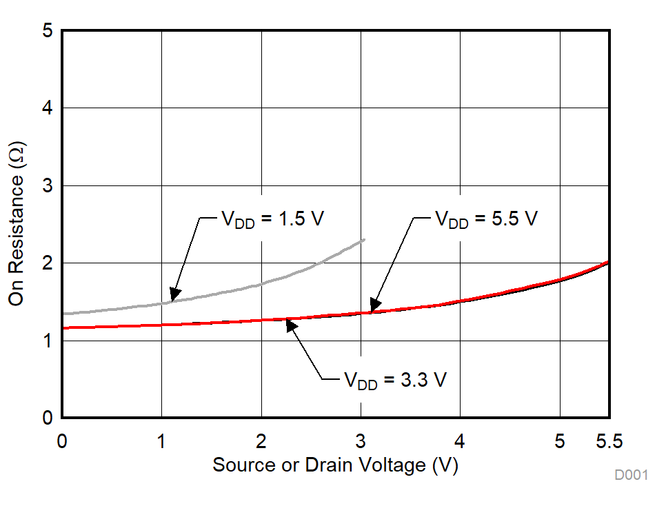
TMUX1574 D001_SCDS391.gif
TA = 25°C
Figure 1. On-Resistance vs Source or Drain Voltage
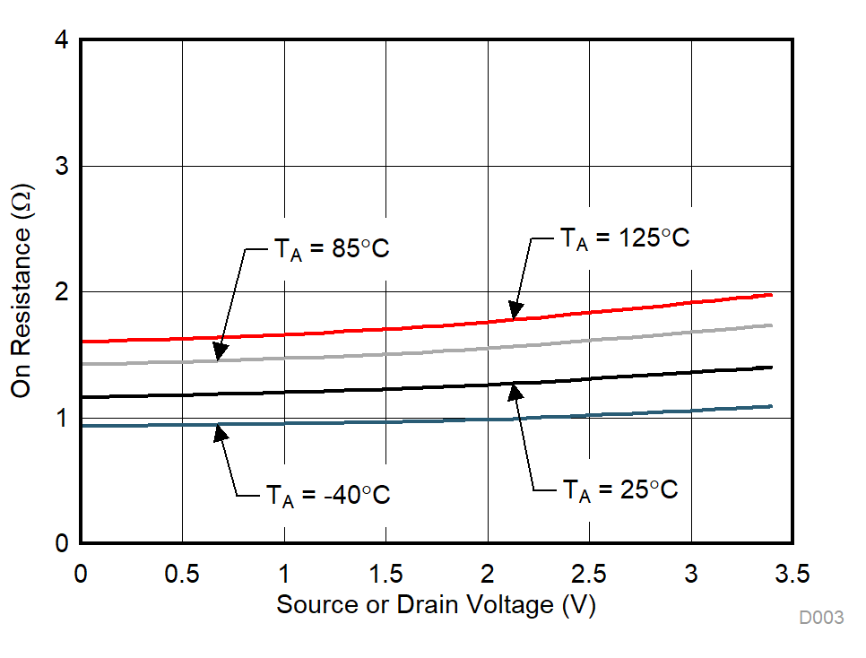
TMUX1574 D003_SCDS391.gif
VDD = 3.3 V
Figure 3. On-Resistance vs Source or Drain Voltage
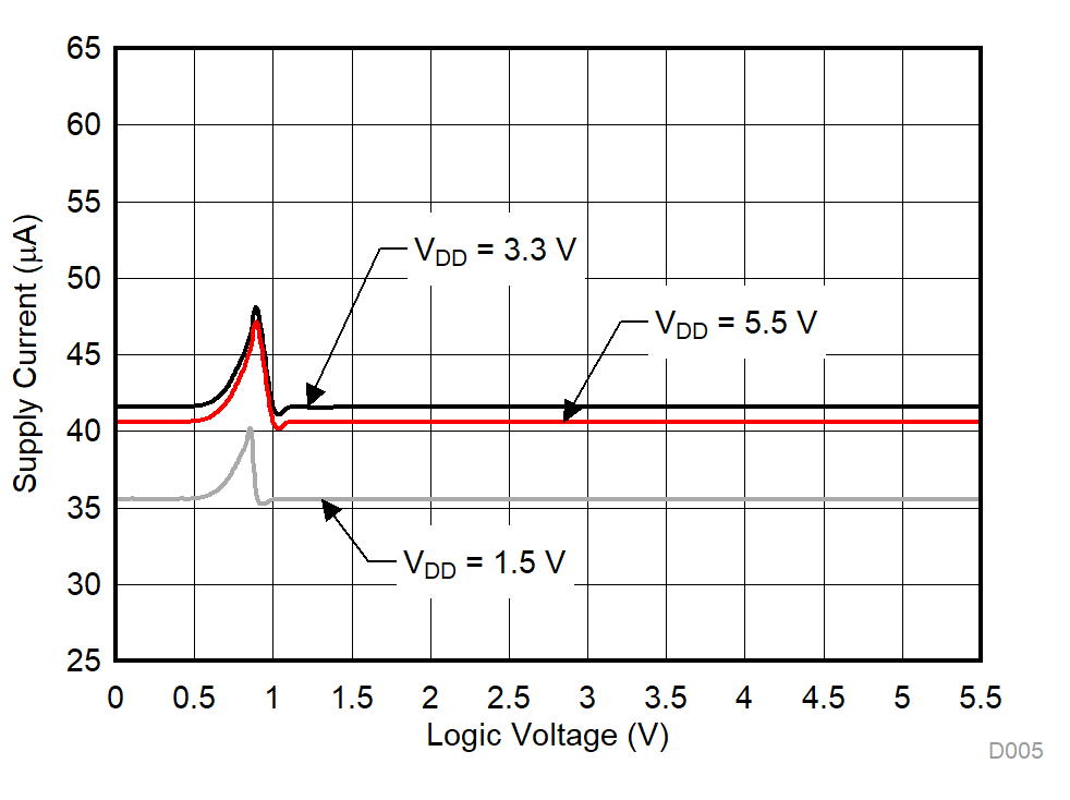
TMUX1574 D005_SCDS391.gif
TA = 25°C
Figure 5. Supply Current vs Logic Voltage
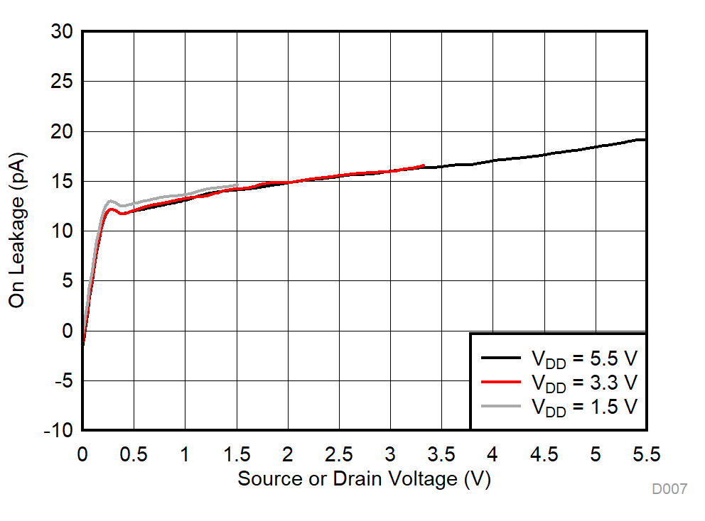
TMUX1574 D007_SCDS391.gif
TA = 25°C
Figure 7. On-Leakage vs Source or Drain Voltage
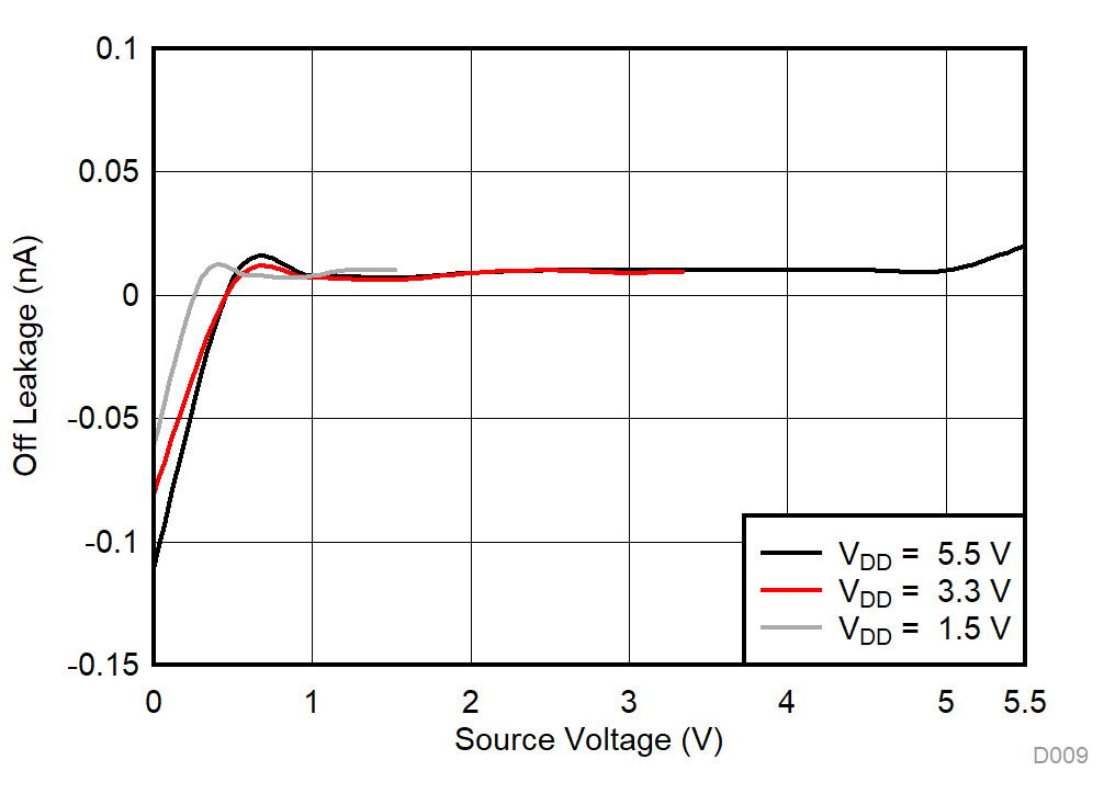
TMUX1574 D009_SCDS391.gif
TA = 25°C
Figure 9. Off-Leakage vs Source or Drain Voltage
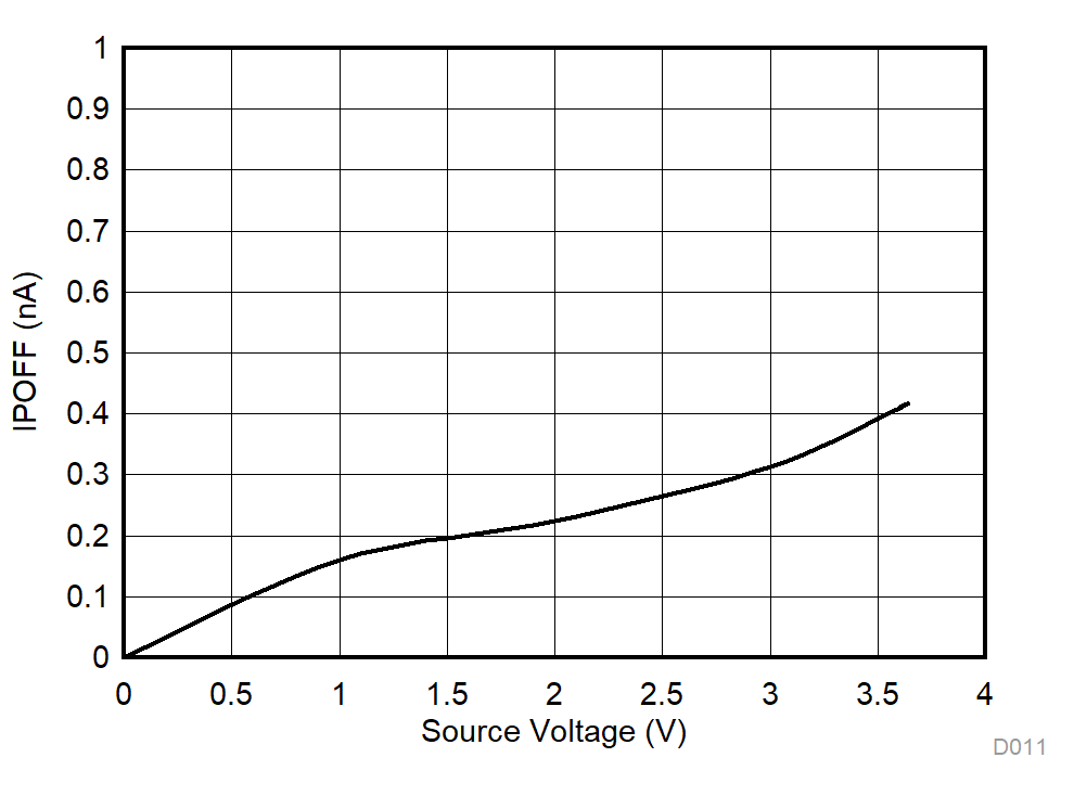
TMUX1574 D011_SCDS391.gif
TA = 25°C
Figure 11. IPOFF Leakage vs Source or Drain Voltage
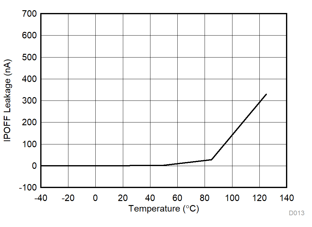
TMUX1574 D013_SCDS391.gif
VSource = 3.6 V
VDrain = 0 V
Figure 13. IPOFF Leakage vs Temperature
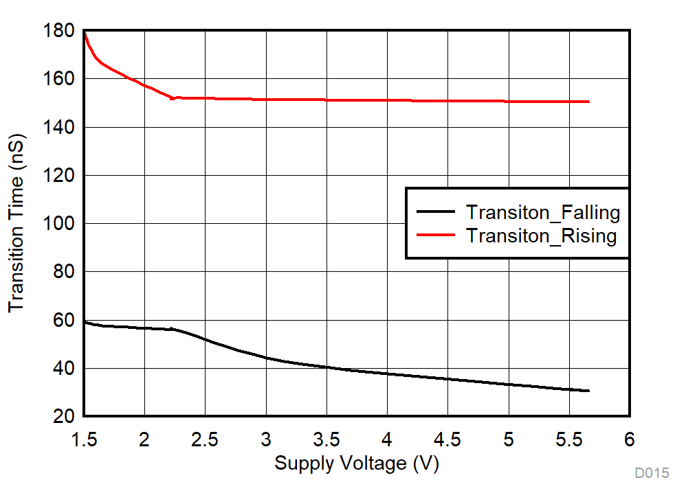
TMUX1574 D015_SCDS391.gif
TA = 25°C
Figure 15. TTRANSITION vs Supply Voltage
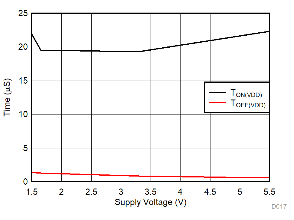
TMUX1574 D017_SCDS391.gif
TA = 25°C
Figure 17. TON (VDD) and TOFF (VDD) vs Supply Voltage
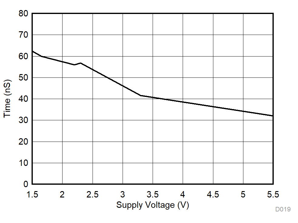
TMUX1574 D019_SCDS391.gif
TA = 25°C
Figure 19. TOFF (EN) vs Supply Voltage
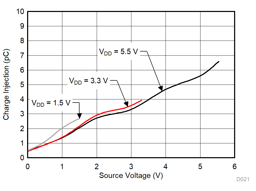
TMUX1574 D021_SCDS391.gif
TA = 25°C
Figure 21. Charge Injection vs Source Voltage
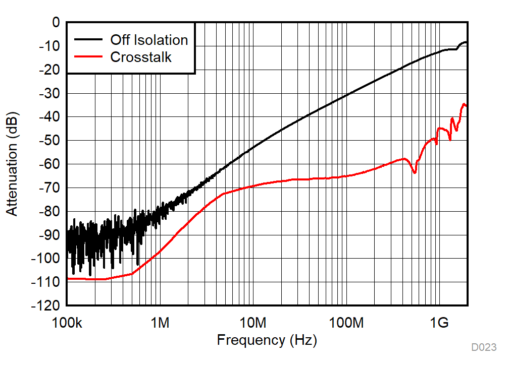
TMUX1574 D023_SCDS391.gif
TA = 25°C
VDD = 3.3 V
Figure 23. Off Isolation and Crosstalk vs Frequency
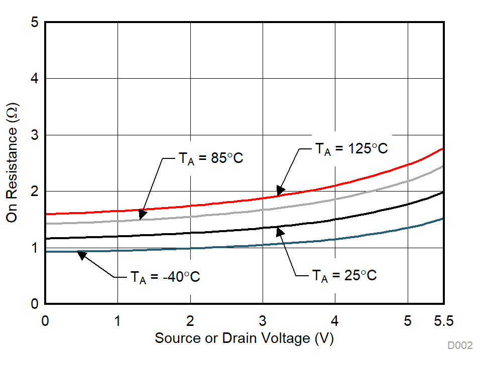
TMUX1574 D002_SCDS391.gif
VDD = 5.5 V
Figure 2. On-Resistance vs Source or Drain Voltage
TMUX1574 D004_SCDS391.gif
VDD = 1.5 V
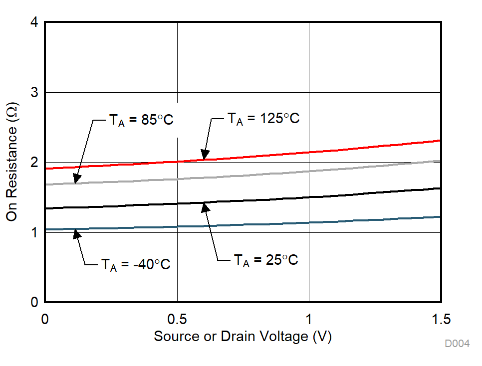
Figure 4. On-Resistance vs Source or Drain Voltage
TMUX1574 D006_SCDS391.gif
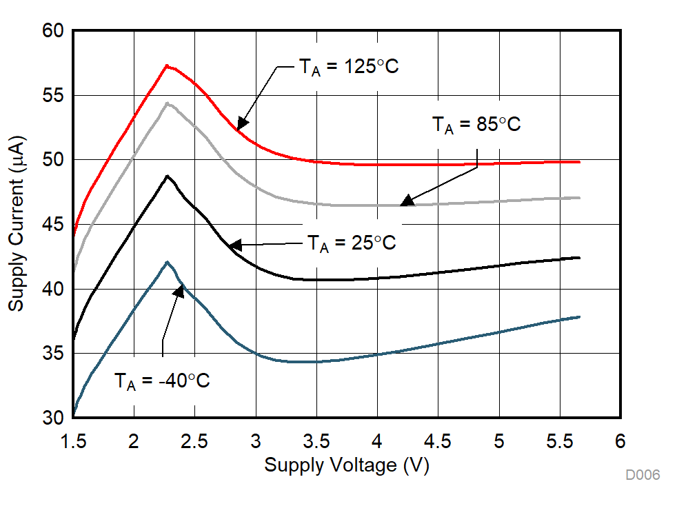
Figure 6. Supply Current vs Supply Voltage
TMUX1574 D008_SCDS391.gif
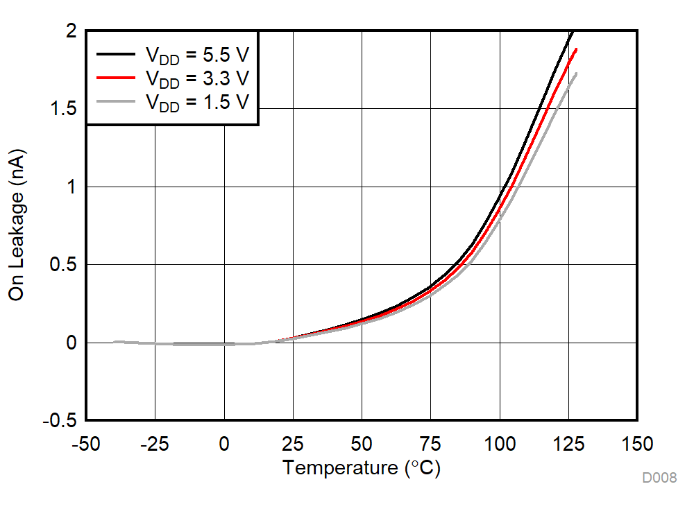
Figure 8. On-Leakage vs Temperature
TMUX1574 D010_SCDS391.gif
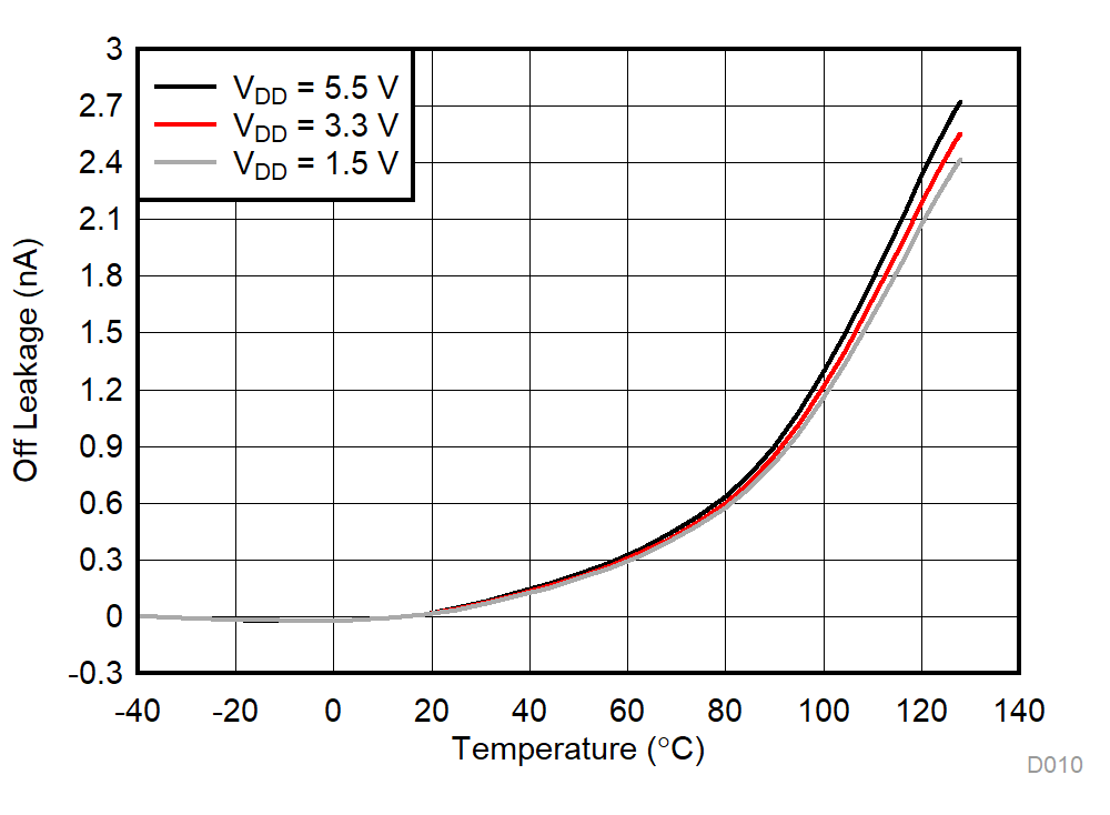
Figure 10. Off-Leakage vs Temperature
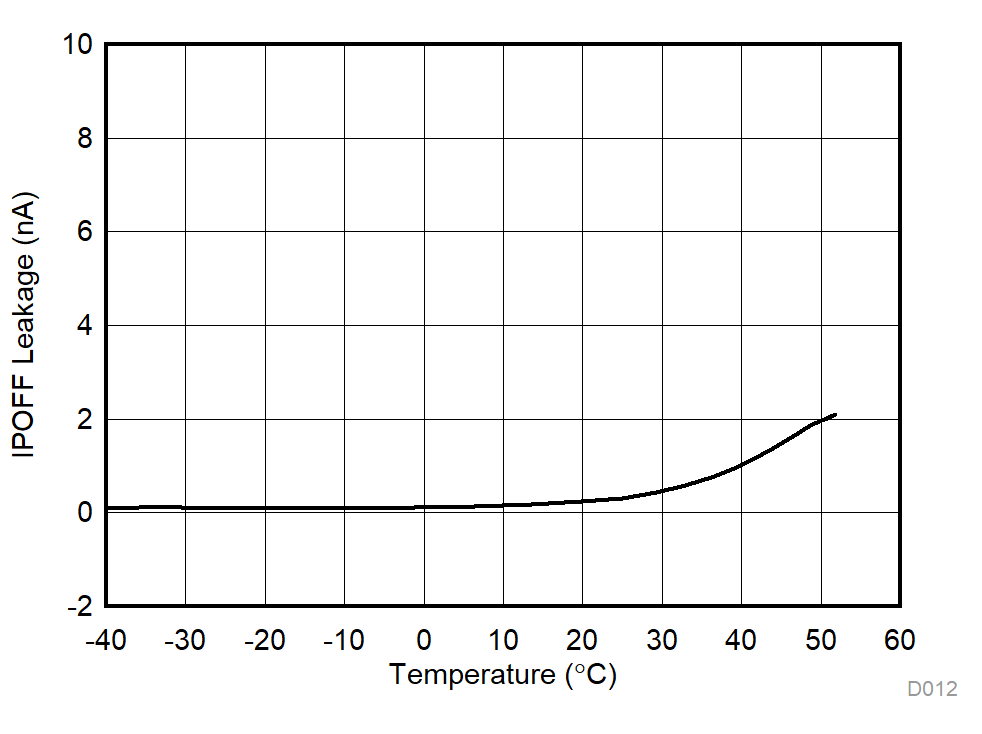
TMUX1574 D012_SCDS391.gif
VSource = 3 V
Figure 12. IPOFF Leakage vs Temperature
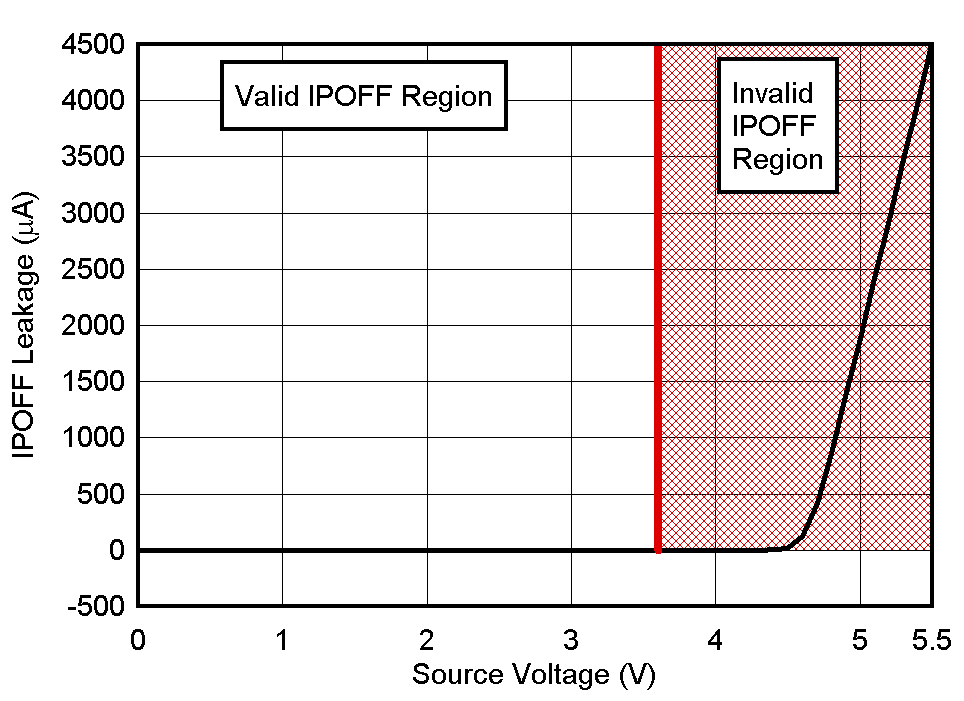
TMUX1574 D014_SCDS391.png
TA = 25°C
RL= 200 Ω
Figure 14. IPOFF Leakage vs Source or Drain Voltage
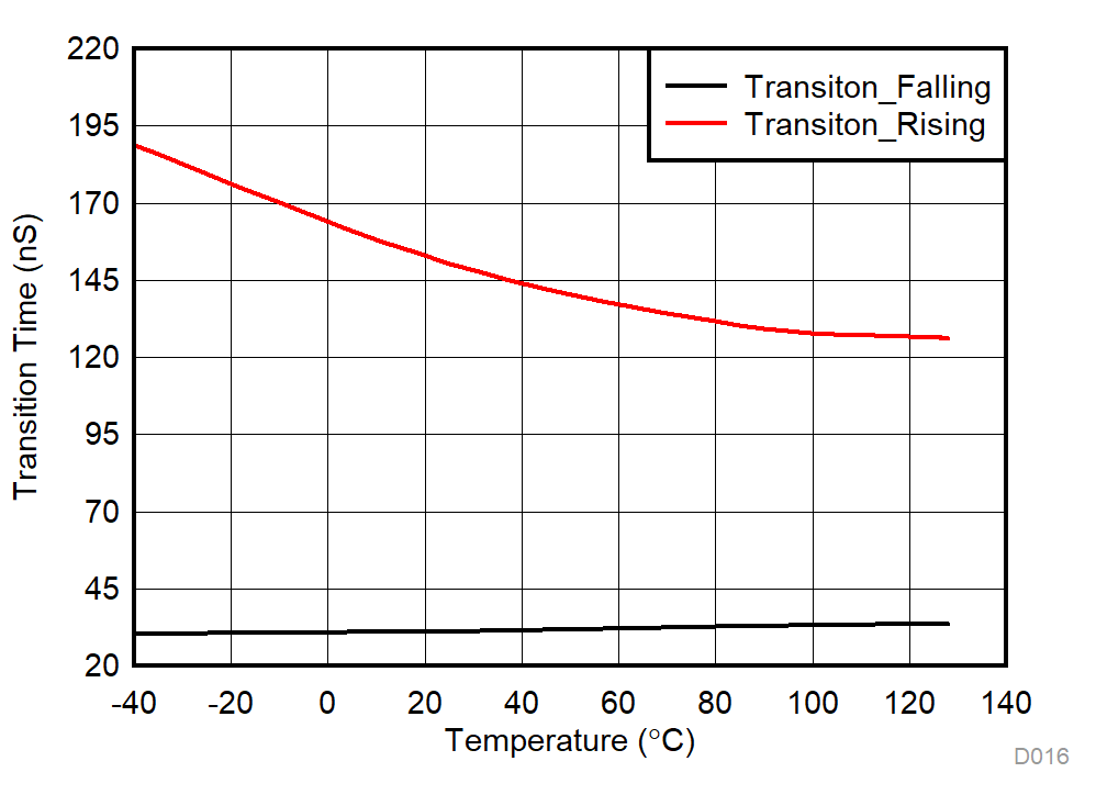
TMUX1574 D016_SCDS391.gif
VDD = 5.5 V
Figure 16. TTRANSITION vs Temperature
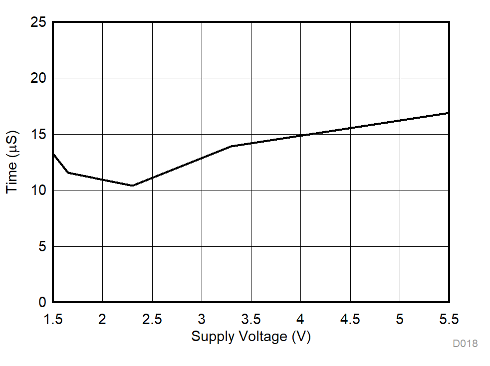
TMUX1574 D018_SCDS391.gif
TA = 25°C
Figure 18. TON (EN) vs Supply Voltage
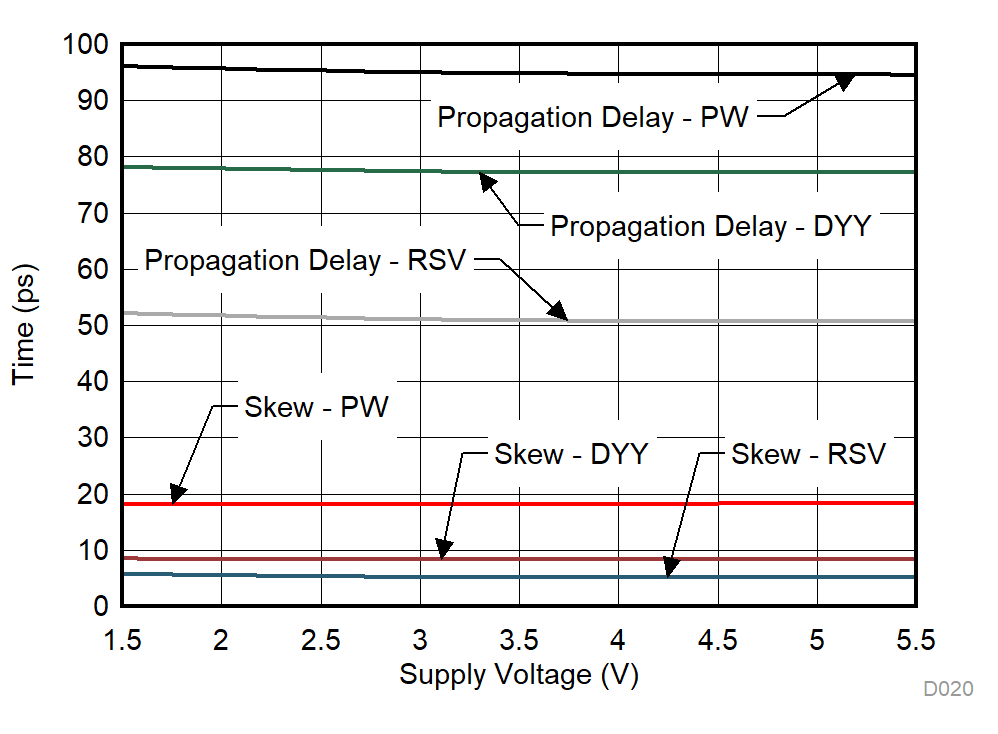
TMUX1574 D020_SCDS391.gif
TA = 25°C
Figure 20. Skew and Propagation Delay vs Supply Voltage
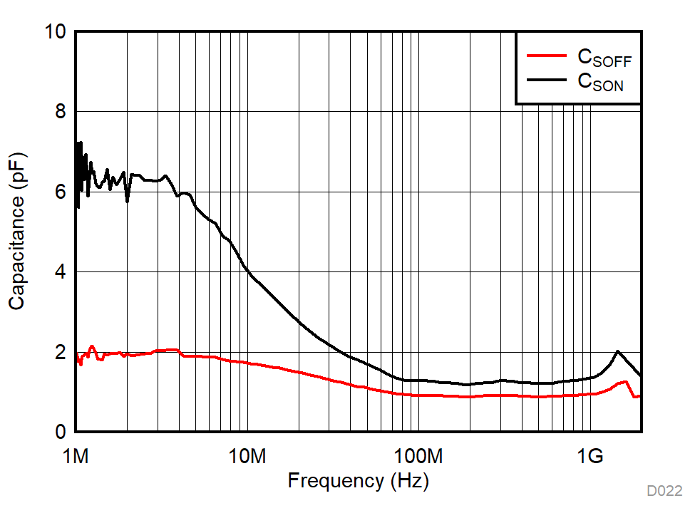
TMUX1574 D022_SCDS391.gif
TA = 25°C
VDD = 1.5 V to 5.5 V
Figure 22. Capacitance vs Frequency
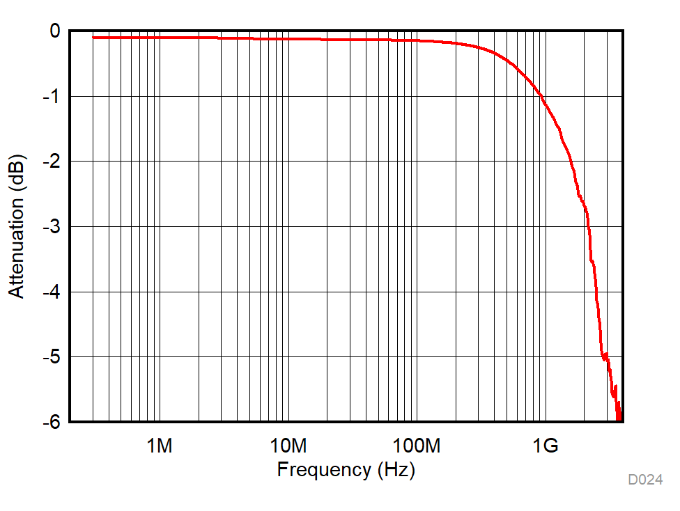
TMUX1574 D024_SCDS391.gif
TA = 25°C
VDD = 1.5 V to 5.5 V
Figure 24. On-Response vs Frequency