SLOS474E August   2005  – March 2016 TPA2005D1-Q1

PRODUCTION DATA.  

  1. Features
  2. Applications
  3. Description
  4. Revision History
  5. Device Comparison Table
  6. Pin Configuration and Functions
  7. Specifications
    1. 7.1 Absolute Maximum Ratings
    2. 7.2 ESD Ratings
    3. 7.3 Recommended Operating Conditions
    4. 7.4 Thermal Information
    5. 7.5 Electrical Characteristics
    6. 7.6 Operating Characteristics
    7. 7.7 Typical Characteristics
  8. Parameter Measurement Information
  9. Detailed Description
    1. 9.1 Overview
    2. 9.2 Functional Block Diagram
    3. 9.3 Feature Description
      1. 9.3.1 Fully Differential Amplifier
        1. 9.3.1.1 Advantages Of Fully Differential Amplifiers
      2. 9.3.2 Efficiency and Thermal Information
      3. 9.3.3 Eliminating the Output Filter With the TPA2005D1-Q1
        1. 9.3.3.1 Effect On Audio
        2. 9.3.3.2 Traditional Class-D Modulation Scheme
        3. 9.3.3.3 TPA2005D1-Q1 Modulation Scheme
        4. 9.3.3.4 Efficiency: Why You Must Use a Filter With The Traditional Class-D Modulation Scheme
        5. 9.3.3.5 Effects Of Applying a Square Wave Into a Speaker
        6. 9.3.3.6 When to Use an Output Filter
    4. 9.4 Device Functional Modes
      1. 9.4.1 Summing Input Signals With the TPA2005D1-Q1
        1. 9.4.1.1 Summing Two Differential Input Signals
        2. 9.4.1.2 Summing A Differential Input Signal And A Single-Ended Input Signal
        3. 9.4.1.3 Summing Two Single-Ended Input Signals
  10. 10Application and Implementation
    1. 10.1 Application Information
    2. 10.2 Typical Application
      1. 10.2.1 TPA2005D1-Q1 With Differential Input
        1. 10.2.1.1 Design Requirements
        2. 10.2.1.2 Detailed Design Procedure
          1. 10.2.1.2.1 Component Selection
          2. 10.2.1.2.2 Input Resistors (RI)
          3. 10.2.1.2.3 Decoupling Capacitor (CS)
        3. 10.2.1.3 Application Curve
      2. 10.2.2 TPA2005D1-Q1 With Differential Input and Input Capacitors
        1. 10.2.2.1 Detailed Design Requirements
          1. 10.2.2.1.1 Input Capacitors (CI)
      3. 10.2.3 TPA2005D1-Q1 With Single-Ended Input
  11. 11Power Supply Recommendations
    1. 11.1 Power Supply Decoupling Capacitors
  12. 12Layout
    1. 12.1 Layout Guidelines
      1. 12.1.1 Component Location
      2. 12.1.2 Trace Width
      3. 12.1.3 8-Pin QFN (DRB) Layout
    2. 12.2 Layout Example
  13. 13Device and Documentation Support
    1. 13.1 Documentation Support
      1. 13.1.1 Related Documentation
    2. 13.2 Community Resource
    3. 13.3 Trademarks
    4. 13.4 Electrostatic Discharge Caution
    5. 13.5 Glossary
  14. 14Mechanical, Packaging, and Orderable Information

Package Options

Mechanical Data (Package|Pins)
Thermal pad, mechanical data (Package|Pins)
Orderable Information

12 Layout

12.1 Layout Guidelines

12.1.1 Component Location

Place all the external components very close to the TPA2005D1-Q1 device. The input resistors need to be very close to the TPA2005D1-Q1 input pins so noise does not couple on the high-impedance nodes between the input resistors and the input amplifier of the TPA2005D1-Q1 device. Placing the decoupling capacitor, CS, close to the TPA2005D1-Q1 device is important for the efficiency of the class-D amplifier. Any resistance or inductance in the trace between the device and the capacitor can cause a loss in efficiency.

12.1.2 Trace Width

Make the high current traces going to pins VDD, GND, VO+ and VO– of the TPA2005D1-Q1 device have a minimum width of 0.7 mm. If these traces are too thin, the TPA2005D1-Q1 performance and output power will decrease. The input traces do not need to be wide, but do need to run side-by-side to enable common-mode noise cancellation.

12.1.3 8-Pin QFN (DRB) Layout

Use the following land pattern for board layout with the 8-pin QFN (DRB) package. Note that the solder paste should use a hatch pattern to fill solder paste at 50% to ensure that there is not too much solder paste under the package.
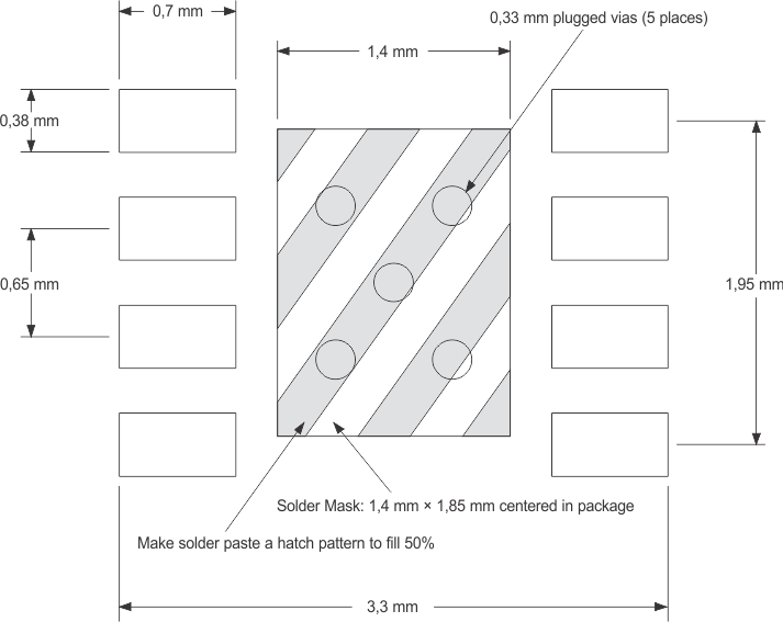
TPA2005D1-Q1 ai_QFN_los474.gif Figure 42. TPA2005D1-Q1 8-Pin QFN (DRB) Board Layout (Top View)

12.2 Layout Example
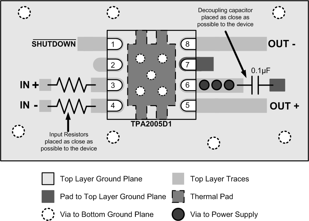
TPA2005D1-Q1 layout_QFN.gif Figure 43. TPA2005D1-Q1 DRB Package Layout Example
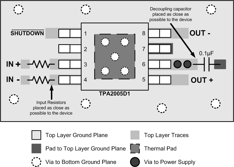
TPA2005D1-Q1 layout_MSOP.gif Figure 44. TPA2005D1-Q1 DGN Package Layout Example