SLOS862B July 2015 – October 2016 TPA3116D2-Q1 , TPA3118D2-Q1
PRODUCTION DATA.
- 1 Features
- 2 Applications
- 3 Description
- 4 Revision History
- 5 Pin Configuration and Functions
- 6 Specifications
-
7 Detailed Description
- 7.1 Overview
- 7.2 Functional Block Diagram
- 7.3
Feature Description
- 7.3.1 Gain Setting and Master and Slave
- 7.3.2 Input Impedance
- 7.3.3 Start-Up and Shutdown Operation
- 7.3.4 PLIMIT Operation
- 7.3.5 GVDD Supply
- 7.3.6 BSPx and BSNx Capacitors
- 7.3.7 Differential Inputs
- 7.3.8 Device Protection System
- 7.3.9 DC-Detect Protection
- 7.3.10 Short-Circuit Protection and Automatic Recovery Feature
- 7.3.11 Thermal Protection
- 7.3.12 TPA311xD2-Q1 Modulation Scheme
- 7.3.13 AM Avoidance EMI Reduction
- 7.4 Device Functional Mode
- 8 Application and Implementation
- 9 Power Supply Recommendations
- 10Layout
- 11Device and Documentation Support
- 12Mechanical, Packaging, and Orderable Information
Package Options
Mechanical Data (Package|Pins)
- DAP|32
Thermal pad, mechanical data (Package|Pins)
- DAP|32
Orderable Information
7 Detailed Description
7.1 Overview
The TPA311xD2-Q1 devices are highly efficient class-D audio amplifiers with integrated 120-mΩ MOSFETs that allow output currents up to 7.5 A. The high efficiency allows the amplifier to provide an excellent audio performance without the need for a bulky heat sink.
The device can be configured for either master or slave operation by using the SYNC pin. Doing so helps to prevent audible beat noise.
7.2 Functional Block Diagram
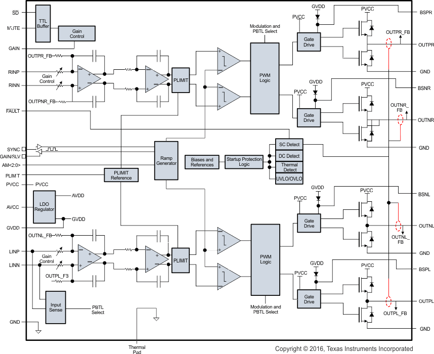
7.3 Feature Description
7.3.1 Gain Setting and Master and Slave
The gain of the TPA311xD2-Q1 family is set by the voltage divider connected to the GAIN/SLV control pin. Master or slave mode is also controlled by the same pin. An internal ADC is used to detect the eight input states. The first four stages set the GAIN in master mode to gains of 20, 26, 32, and 36 dB, respectively, whereas the next four stages set the GAIN in slave mode to gains of 20, 26, 32, and 36 dB, respectively. The gain setting is latched during power up and cannot be changed while device is powered. Table 1 lists the recommended resistor values and the state and gain.
Table 1. Gain and Master or Slave
| MASTER / SLAVE MODE | GAIN | R1 (to GND)(1) | R2 (to GVDD)(1) | INPUT IMPEDANCE |
|---|---|---|---|---|
| Master | 20 dB | 5.6 kΩ | OPEN | 60 kΩ |
| Master | 26 dB | 20 kΩ | 100 kΩ | 30 kΩ |
| Master | 32 dB | 39 kΩ | 100 kΩ | 15 kΩ |
| Master | 36 dB | 47 kΩ | 75 kΩ | 9 kΩ |
| Slave | 20 dB | 51 kΩ | 51 kΩ | 60 kΩ |
| Slave | 26 dB | 75 kΩ | 47 kΩ | 30 kΩ |
| Slave | 32 dB | 100 kΩ | 39 kΩ | 15 kΩ |
| Slave | 36 dB | 100 kΩ | 16 kΩ | 9 kΩ |
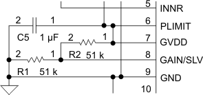 Figure 12. Gain, Master or Slave
In master mode, the SYNC terminal is an output, in slave mode, SYNC terminal is an input for a clock input.
7.3.2 Input Impedance
The input stage of the TPA311xD2-Q1 family is a fully differential input stage, and the input impedance changes with the gain setting from 9 kΩ at 36-dB gain to 60 kΩ at 20-dB gain. Table 1 lists the values from mininimum to maximum gain. The tolerance of the input resistor value is ±20%, so the minimum value is higher than 7.2 kΩ. The inputs must be ac-coupled to minimize the output dc offset and ensure correct ramping of the output voltages during power ON and power OFF. The input ac-coupling capacitor together with the input impedance forms a high-pass filter with the following cutoff frequency:

If a flat bass response is required down to 20 Hz, the recommended cutoff frequency is a tenth of that, 2 Hz. Table 2 lists the recommended ac-coupling capacitors for each gain step. If –3 dB is accepted at 20 Hz, 10 times lower capacitors can used – for example, a 1 µF can be used.
Table 2. Recommended Input AC-Coupling Capacitors
| GAIN | INPUT IMPEDANCE | INPUT CAPACITANCE | HIGH-PASS FILTER |
|---|---|---|---|
| 20 dB | 60 kΩ | 1.5 µF | 1.8 Hz |
| 26 dB | 30 kΩ | 3.3 µF | 1.6 Hz |
| 32 dB | 15 kΩ | 5.6 µF | 2.3 Hz |
| 36 dB | 9 kΩ | 10 µF | 1.8 Hz |
 Figure 13. Input Impedance
The input capacitors used should be a type with low leakage, like quality electrolytic, tantalum, or ceramic. If a polarized type is used, the positive connection should face the input pins, which are biased to 3 Vdc.
7.3.3 Start-Up and Shutdown Operation
The TPA311xD2-Q1 family employs a shutdown mode of operation designed to reduce supply current (ICC) to the absolute minimum level for power conservation during periods of nonuse. The SD input pin should be held high (see Recommended Operating Conditions for SD VIH and VIL levels) during normal operation when the amplifier is in use. Pulling SD low sets the outputs to mute, and the amplifier enters a low-current state. It is not recommended to leave SD unconnected, because amplifier operation would be unpredictable.
For the best power-off pop performance, place the amplifier in the shutdown mode prior to removing the power supply. The gain setting is selected at the end of the start-up cycle. At the end of the start-up cycle, the gain is selected and cannot be changed until the next power up.
7.3.4 PLIMIT Operation
The TPA311xD2-Q1 family has a built-in voltage limiter that can be used to limit the output voltage level below the supply rail, the amplifier simply operates as if it was powered by a lower supply voltage, and thereby limits the output power. Add a resistor divider from GVDD to ground to set the voltage at the PLIMIT pin. An external reference may also be used if tighter tolerance is required. Add a 1-µF capacitor from the PLIMIT pin to ground to ensure stability. It is recommended to connect PLIMIT to GVDD when using 1SPW-modulation mode.
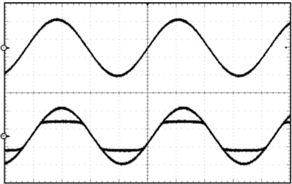 Figure 14. Power Limit Example
The PLIMIT circuit sets a limit on the output peak-to-peak voltage. The limiting is done by limiting the duty cycle to a fixed maximum value. This limit can be thought of as a virtual voltage rail which is lower than the supply connected to PVCC. This virtual rail is approximately 4 times the voltage at the PLIMIT pin. This output voltage can be used to calculate the maximum output power for a given maximum input voltage and speaker impedance.

where
- POUT (10%THD) = 1.25 × POUT (unclipped)
- RL is the load resistance.
- RS is the total series resistance including RDS(on) and output filter resistance.
- VP is the peak amplitude
- VP = 4 × PLIMIT voltage if PLIMIT < 4 × VP
Table 3. Power Limit Example
| PVCC (V) | PLIMIT VOLTAGE (V)(1) | R to GND | R to GVDD | OUTPUT VOLTAGE (Vrms) |
|---|---|---|---|---|
| 24 V | GVDD | Open | Short | 17.9 |
| 24 V | 3.3 | 45 kΩ | 51 kΩ | 12.67 |
| 24 V | 2.25 | 24 kΩ | 51 kΩ | 9 |
| 12 V | GVDD | Open | Short | 10.33 |
| 12 V | 2.25 | 24 kΩ | 51 kΩ | 9 |
| 12 V | 1.5 | 18 kΩ | 68 kΩ | 6.3 |
7.3.5 GVDD Supply
The GVDD supply is used to power the gates of the output full-bridge transistors. The GVDD supply can also be used to supply the PLIMIT and GAIN/SLV voltage dividers. Decouple GVDD with an X5R ceramic 1-µF capacitor to GND. The GVDD supply is not intended to be used for external supply. It is recommended to limit the current consumption by using resistor voltage dividers of 100 kΩ or more for GAIN/SLV and PLIMIT.
7.3.6 BSPx and BSNx Capacitors
The full H-bridge output stages use only NMOS transistors. Therefore, to turn on correctly they require bootstrap capacitors for the high side of each output. A 220-nF ceramic capacitor of quality X5R or better, rated for at least 16 V, must be connected from each output to its corresponding bootstrap input. (See the application circuit diagram in Figure 19.) The bootstrap capacitors connected between the BSxx pins and their corresponding outputs function as a floating power supply for the high-side N-channel power MOSFET gate-drive circuitry. During each high-side switching cycle, the bootstrap capacitors hold the gate-to-source voltage high enough to keep the high-side MOSFETs turned on.
7.3.7 Differential Inputs
The differential input stage of the amplifier cancels any noise that appears on both input lines of the channel. To use the TPA311xD2-Q1 family with a differential source, connect the positive lead of the audio source to the RINP or LINP input and the negative lead from the audio source to the RINN or LINN input. To use the TPA311xD2-Q1 family with a single-ended source, ac-ground the negative input through a capacitor equal in value to the input capacitor on the positive input and apply the audio source to either input. In a single-ended input application, the unused input should be ac-grounded at the audio source instead of at the device input for best noise performance. For good transient performance, the impedance seen at each of the two differential inputs should be the same.
The impedance seen at the inputs should be limited to an RC time constant of 1 ms or less if possible. This is to allow the input dc-blocking capacitors to become completely charged during the 10-ms power-up time. If the input capacitors are not allowed to completely charge, there is some additional sensitivity to component matching which can result in a pop if the input components are not well matched.
7.3.8 Device Protection System
The TPA311xD2-Q1 family contains a complete set of protection circuits to make system design efficient as well as to protect the device against any kind of permanent failures due to short circuits, overload, overtemperature, and undervoltage. The FAULT pin signals if an error is detected according to Table 4:
Table 4. Fault Reporting
| FAULT | TRIGGERING CONDITION (typical value) |
FAULT | ACTION | LATCHED OR SELF-CLEARING |
|---|---|---|---|---|
| Overcurrent | Output short or short to PVCC or GND | Low | Output high impedance | Latched |
| Overtemperature | Tj > 150°C | Low | Output high impedance | Latched |
| Too-high dc offset | DC output voltage | Low | Output high impedance | Latched |
| Undervoltage on PVCC | V(PVCC) < 4.5 V | – | Output high impedance | Self-clearing |
| Overvoltage on PVCC | V(PVCC) > 27 V | – | Output high impedance | Self-clearing |
7.3.9 DC-Detect Protection
The TPA311xD2-Q1 family has circuitry which protects the speakers from dc current, which might occur due to defective capacitors on the input or shorts on the printed circuit board at the inputs. A dc-detect fault is reported on the FAULT pin as a low state. The dc-detect fault also causes the amplifier to shut down by changing the state of the outputs to Hi-Z.
If automatic recovery from the short-circuit protection latch is desired, connect the FAULT pin directly to the SD pin. This allows the FAULT pin function to automatically drive the SD pin low which clears the dc-detect protection latch.
A dc-detect fault is issued when the output differential duty-cycle of either channel exceeds 60% for more than 420 ms at the same polarity. For several values of the supply voltage, Table 5 shows some examples of the typical output offset voltages that trigger dc-detect protection. This feature protects the speaker from large dc currents or ac currents less than 2 Hz. To avoid nuisance faults due to the dc-detect circuit, hold the SD pin low at power up until the signals at the inputs are stable. Also, take care to match the impedance seen at the positive and negative inputs to avoid nuisance dc-detect faults.
Table 5 lists the minimum output offset voltages required to trigger the dc detect. The outputs must remain at or above the voltage listed in the table for more than 420 ms to trigger the dc detect.
Table 5. DC Detect Threshold
| V(PVCC) (V) | VOS - OUTPUT OFFSET VOLTAGE (V) |
|---|---|
| 4.5 | 0.96 |
| 6 | 1.3 |
| 12 | 2.6 |
| 18 | 3.9 |
7.3.10 Short-Circuit Protection and Automatic Recovery Feature
The TPA311xD2-Q1 family has protection from overcurrent conditions caused by a short circuit on the output stage. The short-circuit protection fault is reported on the FAULT pin as a low state. The amplifier outputs are switched to a high-impedance state when the short-circuit protection latch is engaged. The latch can be cleared by cycling the SD pin through the low state.
If automatic recovery from the short-circuit protection latch is desired, connect the FAULT pin directly to the SD pin. This allows the FAULT pin function to automatically drive the SD pin low, which clears the short-circuit protection latch.
In systems where a possibility of a permanent short from the output to PVDD or to a high-voltage battery like a car battery can occur, pull the MUTE pin low with the FAULT signal and an inverting transistor to ensure a high-Z restart, as shown in Figure 15.
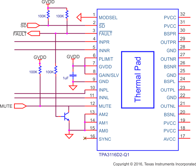 Figure 15. MUTE Driven by Inverted FAULT
7.3.11 Thermal Protection
Thermal protection on the TPA311xD2-Q1 family prevents damage to the device when the internal die temperature exceeds 150°C. There is a ±15°C tolerance on this trip point from device to device. Once the die temperature exceeds the thermal trip point, the device enters the shutdown state and the outputs are disabled. This is a latched fault.
Thermal protection faults are reported on the FAULT pin as a low state.
If automatic recovery from the thermal protection latch is desired, connect the FAULT pin directly to the SD pin. This allows the FAULT pin function to automatically drive the SD pin low, which clears the thermal protection latch.
7.3.12 TPA311xD2-Q1 Modulation Scheme
The TPA311xD2-Q1 family has the option of running in either BD modulation or 1SPW modulation; this is set by the MODSEL pin.
7.3.12.1 MODSEL = GND: BD Modulation
Each output is switching from 0 volts to the supply voltage. The OUTPx and OUTNx are in phase with each other with no input so that there is little or no current in the speaker. The duty cycle of OUTPx is greater than 50% and OUTNx is less than 50% for positive output voltages. The duty cycle of OUTPx is less than 50% and OUTNx is greater than 50% for negative output voltages. The voltage across the load sits at 0 V throughout most of the switching period, reducing the switching current, which reduces any I2R losses in the load.
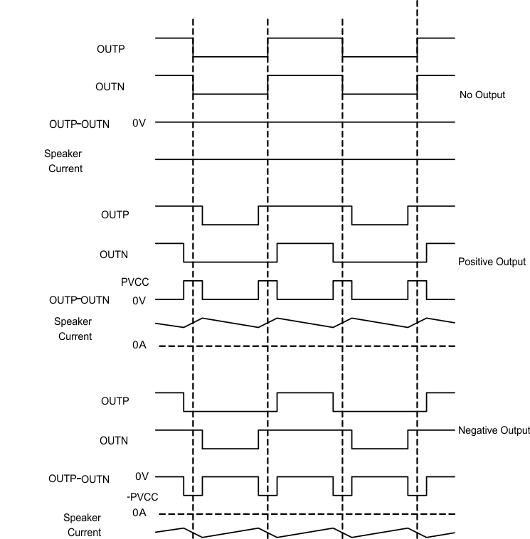 Figure 16. BD Mode Modulation
7.3.12.2 MODSEL = HIGH: 1SPW Modulation
The 1SPW mode alters the normal modulation scheme in order to achieve higher efficiency with a slight penalty in THD degradation, and more attention required in the output filter selection. In 1SPW mode, the outputs operate at approximately 15% modulation during idle conditions. When an audio signal is applied, one output decreases and one increases. The decreasing output signal quickly rails to GND at which point all the audio modulation takes place through the rising output. The result is that only one output is switching during a majority of the audio cycle. Efficiency is improved in this mode due to the reduction of switching losses. The THD penalty in 1SPW mode is minimized by the high-performance feedback loop. The resulting audio signal at each half-output has a discontinuity each time the output rails to GND. This can cause ringing in the audio reconstruction filter unless care is taken in the selection of the filter components and type of filter used.
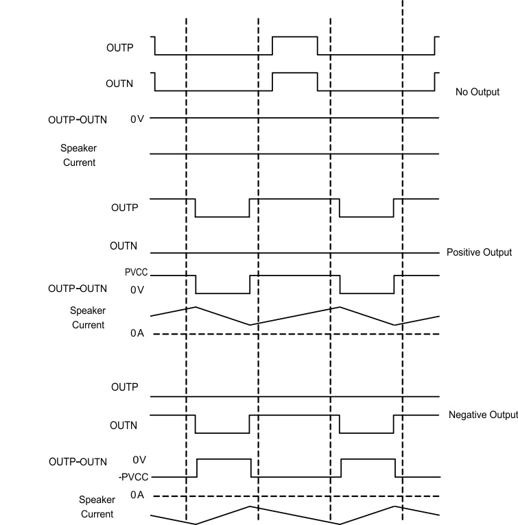 Figure 17. 1SPW Mode Modulation
7.3.13 AM Avoidance EMI Reduction
To reduce interference in the AM radio band, the TPA3116D2-Q1 has the ability to change the switching frequency via the AM[2:0] pins. The recommended frequencies are listed in Table 6. The fundamental frequency and its second harmonic straddle the AM radio band listed. This eliminates the tones that can be present due to the switching frequency being demodulated by the AM radio.
Table 6. AM Frequencies
| US | EUROPEAN | ||||
|---|---|---|---|---|---|
| AM FREQUENCY (kHz) | AM FREQUENCY (kHz) | SWITCHING FREQUENCY (kHz) | AM2 | AM1 | AM0 |
| 522–540 | |||||
| 540–917 | 540–914 | 500 | 0 | 0 | 1 |
| 917–1125 | 914–1122 | 600 (or 400) | 0 | 1 | 0 |
| 0 | 0 | 0 | |||
| 1125–1375 | 1122–1373 | 500 | 0 | 0 | 1 |
| 1375–1547 | 1373–1548 | 600 (or 400) | 0 | 1 | 0 |
| 0 | 0 | 0 | |||
| 1547–1700 | 1548–1701 | 600 (or 500) | 0 | 1 | 0 |
| 0 | 0 | 1 | |||
7.4 Device Functional Mode
7.4.1 Mono Mode (PBTL)
The TPA311xD2-Q1 family can be connected in MONO mode enabling up to 100-W output power. This is done by:
- Connecting INPL and INNL directly to ground (without capacitors) to set the device in mono mode during power up
- Connecting OUTPR and OUTNR together for the positive speaker terminal and OUTNL and OUTPL together for the negative terminal
- Applying the analog input signal to INPR and INNR
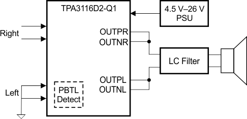 Figure 18. Mono Mode (PBTL)