SLOS862B July 2015 – October 2016 TPA3116D2-Q1 , TPA3118D2-Q1
PRODUCTION DATA.
- 1 Features
- 2 Applications
- 3 Description
- 4 Revision History
- 5 Pin Configuration and Functions
- 6 Specifications
-
7 Detailed Description
- 7.1 Overview
- 7.2 Functional Block Diagram
- 7.3
Feature Description
- 7.3.1 Gain Setting and Master and Slave
- 7.3.2 Input Impedance
- 7.3.3 Start-Up and Shutdown Operation
- 7.3.4 PLIMIT Operation
- 7.3.5 GVDD Supply
- 7.3.6 BSPx and BSNx Capacitors
- 7.3.7 Differential Inputs
- 7.3.8 Device Protection System
- 7.3.9 DC-Detect Protection
- 7.3.10 Short-Circuit Protection and Automatic Recovery Feature
- 7.3.11 Thermal Protection
- 7.3.12 TPA311xD2-Q1 Modulation Scheme
- 7.3.13 AM Avoidance EMI Reduction
- 7.4 Device Functional Mode
- 8 Application and Implementation
- 9 Power Supply Recommendations
- 10Layout
- 11Device and Documentation Support
- 12Mechanical, Packaging, and Orderable Information
Package Options
Mechanical Data (Package|Pins)
- DAP|32
Thermal pad, mechanical data (Package|Pins)
- DAP|32
Orderable Information
6 Specifications
6.1 Absolute Maximum Ratings
over operating ambient temperature range (unless otherwise noted)(1)| MIN | MAX | UNIT | ||
|---|---|---|---|---|
| Supply voltage, VCC | PVCC, AVCC | –0.3 | 30 | V |
| Input voltage, VI | INPL, INNL, INPR, INNR | –0.3 | 6.3 | V |
| PLIMIT, GAIN/SLV, SYNC | –0.3 | GVDD + 0.3 | V | |
| AM0, AM1, AM2, MUTE, SD, MODSEL | –0.3 | PVCC + 0.3 | V | |
| Slew rate, maximum(2) | AM0, AM1, AM2, MUTE, SD, MODSEL | 10 | V/ms | |
| Operating ambient temperature, TA | –40 | 125 | °C | |
| Operating junction temperature range, TJ | –40 | 150 | °C | |
| Storage temperature range, Tstg | –40 | 125 | °C | |
(1) Stresses beyond those listed under Absolute Maximum Ratings may cause permanent damage to the device. These are stress ratings only, and functional operation of the device at these or any other conditions beyond those indicated under Recommended Operating Conditions is not implied. Exposure to absolute-maximum-rated conditions for extended periods may affect device reliability.
(2) 100-kΩ series resistor is needed if maximum slew rate is exceeded.
6.2 ESD Ratings
| VALUE | UNIT | ||||
|---|---|---|---|---|---|
| V(ESD) | Electrostatic discharge | Human-body model (HBM), per AEC Q100-002(1) | ±2000 | V | |
| Charged-device model (CDM), per AEC Q100-011 | All pins | ±450 | |||
| Corner pins (1, 16, 17, and 32) | ±450 | ||||
(1) AEC Q100-002 indicates that HBM stressing shall be in accordance with the ANSI/ESDA/JEDEC JS-001 specification.
6.3 Recommended Operating Conditions
over operating ambient temperature range (unless otherwise noted)| MIN | NOM | MAX | UNIT | ||||
|---|---|---|---|---|---|---|---|
| VCC | Supply voltage | PVCC, AVCC | 4.5 | 26 | V | ||
| VIH | High-level input voltage | AM0, AM1, AM2, MUTE, SD, SYNC, MODSEL | 2 | V | |||
| VIL | Low-level input voltage | AM0, AM1, AM2, MUTE, SD, SYNC, MODSEL | 0.8 | V | |||
| VOL | Low-level output voltage | FAULT, RPULLUP = 100 kΩ, V(PVCC) = 26 V | 0.8 | V | |||
| IIH | High-level input current | AM0, AM1, AM2, MUTE, SD, MODSEL (VI = 2 V, VCC = 18 V) | 50 | µA | |||
| RL | Minimum load impedance | Output filter: L = 10 µH, C = 680 nF, BTL | 3.2 | 4 | Ω | ||
| Output filter: L = 10 µH, C = 1 µF, PBTL | 1.6 | ||||||
| Lo | Output-filter inductance | Minimum output filter inductance under short-circuit condition | 1 | µH | |||
6.4 Thermal Information
| THERMAL METRIC(1) | TPA3116D2-Q1 | TPA3118D2-Q1 | UNIT | |
|---|---|---|---|---|
| DAD | DAP | |||
| 32 PINS | 32 PINS | |||
| RθJA | Junction-to-ambient thermal resistance | 44.7(2) | 32.4 | °C/W |
| RθJC(top) | Junction-to-case (top) thermal resistance | 1.2 | 17.2 | °C/W |
| RθJB | Junction-to-board thermal resistance | 21.5 | 17.3 | °C/W |
| ψJT | Junction-to-top characterization parameter | 1.2 | 0.4 | °C/W |
| ψJB | Junction-to-board characterization parameter | 21 | 17.2 | °C/W |
| RθJC(bot) | Junction-to-case (bottom) thermal resistance | N/A | 1 | °C/W |
(1) For more information about traditional and new thermal metrics, see the Semiconductor and IC Package Thermal Metrics application report.
(2) Modeled with a 15-mm × 15-mm × 2-mm copper heat slug heat sink. A better heat sink or airflow would yield a much better RθJA. Perfect heat sink results could be as low as RθJC(top) = 1.2 ºC/W.
6.5 DC Electrical Characteristics
TA = 25°C, AVCC = PVCC = 12 V to 24 V, RL = 4 Ω (unless otherwise noted)| PARAMETER | TEST CONDITIONS | MIN | TYP | MAX | UNIT | ||
|---|---|---|---|---|---|---|---|
| | VOS | | Class-D output offset voltage (measured differentially) | VI = 0 V, gain = 36 dB | 1.5 | 15 | mV | ||
| ICC | Quiescent supply current | SD = 2 V, no load or filter, V(PVCC) = 12 V | 20 | 35 | mA | ||
| SD = 2 V, no load or filter, V(PVCC) = 24 V | 32 | 50 | |||||
| ICC(SD) | Quiescent supply current in shutdown mode | SD = 0.8 V, no load or filter, V(PVCC) = 12 V | <50 | µA | |||
| SD = 0.8 V, no load or filter, V(PVCC) = 24 V | 50 | 400 | |||||
| rDS(on) | Drain-source on-state resistance, measured pin-to-pin | V(PVCC) = 21 V, IO = 500 mA, TJ = 25°C | 120 | mΩ | |||
| G | Gain (BTL) | R1 = open, R2 = 20 kΩ | 19 | 20 | 21 | dB | |
| R1 = 100 kΩ, R2 = 20 kΩ | 25 | 26 | 27 | ||||
| R1 = 100 kΩ, R2 = 39 kΩ | 31 | 32 | 33 | dB | |||
| R1 = 75 kΩ, R2 = 47 kΩ | 35 | 36 | 37 | ||||
| G | Gain (SLV) | R1 = 51 kΩ, R2 = 51 kΩ | 19 | 20 | 21 | dB | |
| R1 = 47 kΩ, R2 = 75 kΩ | 25 | 26 | 27 | ||||
| R1 = 39 kΩ, R2 = 100 kΩ | 31 | 32 | 33 | dB | |||
| R1 = 16 kΩ, R2 = 100 kΩ | 35 | 36 | 37 | ||||
| ton | Turn-on time | V(SD) = 2 V | 10 | ms | |||
| toff | Turn-off time | V(SD) = 0.8 V | 2 | µs | |||
| GVDD | Gate drive supply | I(GVDD) < 200 µA | 6.4 | 6.9 | 7.4 | V | |
| VO | Output voltage maximum under PLIMIT control | V(PLIMIT) = 2 V; VI = 1 Vrms | 6.75 | 7.9 | 8.75 | V | |
6.6 AC Electrical Characteristics
TA = 25°C, AVCC = PVCC = 12 V to 24 V, RL = 4 Ω (unless otherwise noted)| PARAMETER | TEST CONDITIONS | MIN | TYP | MAX | UNIT | |
|---|---|---|---|---|---|---|
| KSVR | Power supply ripple rejection | 200 mVPP ripple at 1 kHz, gain = 20 dB, inputs ac-coupled to GND | –70 | dB | ||
| PO | Continuous output power | THD+N = 10%, f = 1 kHz, V(PVCC) = 14.4 V | 25 | W | ||
| THD+N = 10%, f = 1 kHz, V(PVCC) = 21 V | 50 | |||||
| THD+N | Total harmonic distortion + noise | VCC = 21 V, f = 1 kHz, PO = 25 W (half-power) | 0.1% | |||
| Vn | Output integrated noise | 20 Hz to 22 kHz, A-weighted filter, gain = 20 dB | 65 | µV | ||
| –80 | dBV | |||||
| Crosstalk | VO = 1 Vrms, gain = 20 dB, f = 1 kHz | –100 | dB | |||
| SNR | Signal-to-noise ratio | Maximum output at THD+N < 1%, f = 1 kHz, gain = 20 dB, A-weighted | 102 | dB | ||
| fOSC | Oscillator frequency | AM[2:0] = 000 | 376 | 400 | 424 | kHz |
| AM[2:0] = 001 | 470 | 500 | 530 | |||
| AM[2:0] = 010 | 564 | 600 | 636 | |||
| AM[2:0] = 011 | 940 | 1000 | 1060 | |||
| AM[2:0] = 100 | 1128 | 1200 | 1278 | |||
| AM[2:0] = 101 | Reserved | |||||
| AM[2:0] = 110 | ||||||
| AM[2:0] = 111 | ||||||
| Thermal trip point | 150 | °C | ||||
| Thermal hysteresis | 15 | °C | ||||
| Overcurrent trip point | 7.5 | A | ||||
6.7 Timing Requirements
| MIN | NOM | MAX | UNIT | ||
|---|---|---|---|---|---|
| td | Delay from MUTE rising to SD falling | 1.4 | s | ||
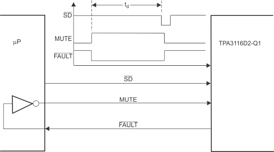 Figure 1. Timing Requirement for SD
6.8 Typical Characteristics
fs = 400 kHz, BD mode (unless otherwise noted)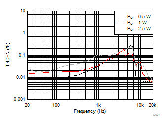
| Gain = 26 dB | PVCC = 6 V | TA = 25°C |
| RL = 4 Ω | 10-µH + 0.68-µF filter | |
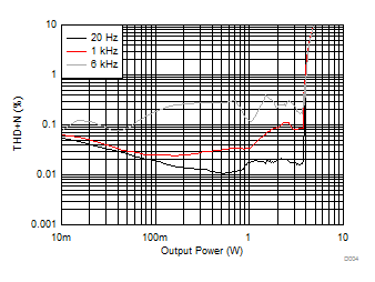
| Gain = 26 dB | PVCC = 6 V | TA = 25°C |
| RL = 4 Ω | 10-µH + 0.68-µF filter | |
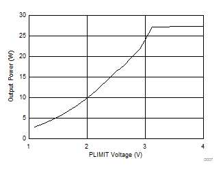
| Gain = 26 dB | PVCC = 14.4 V | TA = 25°C |
| RL = 4 Ω | 10-µH + 0.68-µF filter |
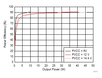
| Gain = 26 dB | TA = 25°C | RL = 4 Ω |
| 10-µH + 0.68-µF filter | ||
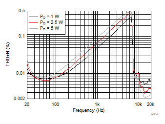
| Gain = 26 dB | PVCC = 14.4 V | TA = 25°C |
| RL = 4 Ω | 22-µH + 1-µF filter | |
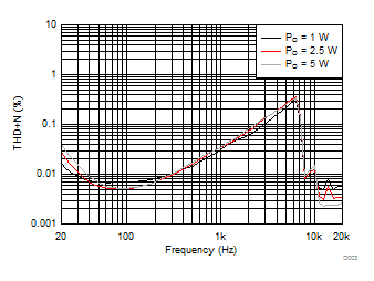
| Gain = 26 dB | PVCC = 14.4 V | TA = 25°C |
| RL = 4 Ω | 10-µH + 0.68-µF filter | |
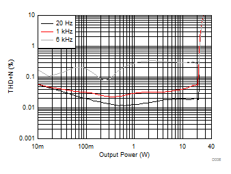
| Gain = 26 dB | PVCC = 14.4 V | TA = 25°C |
| RL = 4 Ω | 10-µH + 0.68-µF filter | |
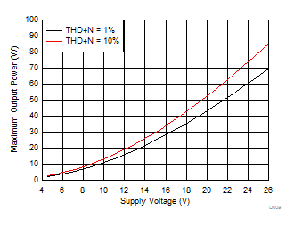
| Gain = 26 dB | TA = 25°C | RL = 4 Ω |
| 10-µH + 0.68-µF filter | ||
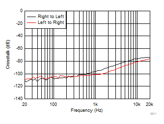
| Gain = 26 dB | PVCC = 12 V | TA = 25°C |
| RL = 4 Ω | 10-µH + 0.68-µF filter | |
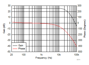
| PVCC = 14.4 V | TA = 25°C | RL = 4 Ω |
| 22-µH + 3.3-µF filter | ||