SLASEE9B September 2017 – December 2017 TPA3221
PRODUCTION DATA.
- 1 Features
- 2 Applications
- 3 Description
- 4 Revision History
- 5 Device Comparison Table
- 6 Pin Configuration and Functions
-
7 Specifications
- 7.1 Absolute Maximum Ratings
- 7.2 ESD Ratings
- 7.3 Recommended Operating Conditions
- 7.4 Thermal Information
- 7.5 Electrical Characteristics
- 7.6 Audio Characteristics (BTL)
- 7.7 Audio Characteristics (PBTL)
- 7.8 Typical Characteristics, BTL Configuration, AD-mode
- 7.9 Typical Characteristics, PBTL Configuration, AD-mode
- 8 Parameter Measurement Information
-
9 Detailed Description
- 9.1 Overview
- 9.2 Functional Block Diagrams
- 9.3 Feature Description
- 9.4
Device Functional Modes
- 9.4.1 Powering Up
- 9.4.2 Powering Down
- 9.4.3 Device Reset
- 9.4.4 Device Soft Mute
- 9.4.5
Device Protection System
- 9.4.5.1 Overload and Short Circuit Current Protection
- 9.4.5.2 Signal Clipping and Pulse Injector
- 9.4.5.3 DC Speaker Protection
- 9.4.5.4 Pin-to-Pin Short Circuit Protection (PPSC)
- 9.4.5.5 Overtemperature Protection OTW and OTE
- 9.4.5.6 Undervoltage Protection (UVP), Overvoltage Protection (OVP) and Power-on Reset (POR)
- 9.4.5.7 Fault Handling
- 10Application and Implementation
- 11Power Supply Recommendations
- 12Layout
- 13Device and Documentation Support
- 14Mechanical, Packaging, and Orderable Information
Package Options
Mechanical Data (Package|Pins)
- DDV|44
Thermal pad, mechanical data (Package|Pins)
- DDV|44
Orderable Information
1 Features
- Wide 7-V to 30-V Supply Voltage Operation
- Stereo (2 x BTL) and Mono (1 x PBTL) Operation
- Output Power at 10% THD+N
- 105-W Stereo into 4 Ω in BTL Configuration
- 112-W Stereo into 3 Ω in BTL Configuration
- 208-W Mono into 2 Ω in PBTL Configuration
- Output Power at 1% THD+N
- 88-W Stereo into 4 Ω in BTL Configuration
- 100-W Stereo into 3 Ω in BTL Configuration
- 170-W Mono into 2 Ω in PBTL Configuration
- 5-V Gate Drive or Built-in LDO for Optional Single-Supply Operation
- Closed-Loop Feedback Design
- Signal Bandwidth up to 100 kHz for High-Frequency Content From HD Sources
- 0.02% THD+N at 1 W into 4 Ω
- 60-dB PSRR (BTL, No Input Signal)
- <75-µV Output Noise (A-Weighted)
- >108-dB SNR (A-Weighted)
- AD or HEAD Modulation Schemes
- Low-Power Operating Modes
- Standby Modes: Mute and < 1 mA Shutdown
- Low Idle-Current HEAD Modulation Scheme
- Single-Channel BTL Operation
- Multiple Input Options to Simplify Pre-Amp Design
- Differential or Single-Ended Analog Inputs
- Selectable Gains: 18 dB, 24 dB, 30 dB, 34 dB
- Integrated Protection: Undervoltage, Overvoltage, Cycle-by-cycle Current Limit, Short Circuit, Clipping Detection, Overtemperature Warning and Shutdown, and DC Speaker Protection
- 90% Efficient Class-D Operation (4 Ω)
- Pin-Compatible Family of Devices with Voltage and Power-Level Options
2 Applications
- Wireless and Powered Speakers
- Soundbars
- Subwoofers
- Bookshelf Stereo Systems
- Professional and Public Address (PA) Speakers
3 Description
TPA3221 is a high-power Class-D amplifier that enables efficient operation at full-power, idle and standby. The device features closed-loop feedback with a bandwidth up to 100 kHz, which provides low distortion across the audio band and delivers excellent sound quality. The device operates with either AD or low idle-current HEAD (High Efficient AD mode) modulation, and can drive up to 2 x 10⁵ W into 4-Ω load or 1 x 208 W into 2-Ω load.
The TPA3221 features a single-ended or differential analog-input interface that supports up to 2 VRMS with four selectable gains: 18 dB, 24 dB, 30 dB and 34 dB. The TPA3221 also achieves >90% efficiency, low idle power (<0.25 W) and ultra-low standby power (<0.1 W). This is made possible through the use of 70-mΩ MOSFETs, an optimized gate drive scheme and low-power operating modes. TPA3221 includes a built-in LDO for easy integration in single-power-supply systems. To further simplify the design, the device integrates essential protection features including undervoltage, overvoltage, cycle-by-cycle current limit, short circuit, clipping detection, overtemperature warning and shutdown, as well as DC speaker protection.
Device Information(1)
| PART NUMBER | PACKAGE | BODY SIZE (NOM) |
|---|---|---|
| TPA3221 | HTSSOP (44) | 6.10 mm x 14.00 mm |
- For all available packages, see the orderable addendum at the end of the datasheet.
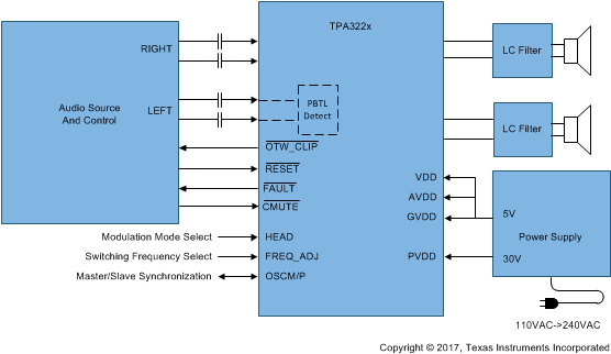
Simplified Schematic

4 Revision History
Changes from A Revision (November 2017) to B Revision
- Changed OUT_P To: OUT1_P for 1 x BTL in Table 1 Go
- Added pins OSCM, OSCP to the Interface pins in the Absolute Maximun Ratings tableGo
- Changed the TJ MIN value From: 0°C To –40°C in the Absolute Maximun Ratings tableGo
- Deleted TJ Junction Temperature from the Recommended Operating Conditions tableGo
- Changed the capacitor on IN1_P, IN2_P and IN1_M, IN2_M From: 10µF To: 1µF in Figure 50Go
- Changed the capacitor on IN1_P and IN1_M From: 10µF To: 1µF in Figure 51Go
- Changed the capacitor on IN1_P and IN1_M From: 10µF To: 1µF in Figure 52Go
Changes from * Revision (September 2017) to A Revision
- Changed From: Advanced Information To: Production DataGo