SLOS821B June 2013 – September 2014 TPA6133A2
PRODUCTION DATA.
- 1 Features
- 2 Applications
- 3 Description
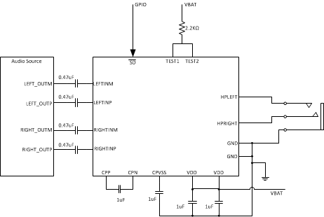
- 4 Simplified Application Diagram
- 5 Revision History
- 6 Pin Configuration and Functions
- 7 Specification
- 8 Detailed Description
- 9 Application and Implementation
- 10Power Supply Recommendations
- 11Layout
- 12Device and Documentation Support
- 13Mechanical, Packaging, and Orderable Information
Package Options
Mechanical Data (Package|Pins)
- RTJ|20
Thermal pad, mechanical data (Package|Pins)
- RTJ|20
Orderable Information
1 Features
- DirectPath™ Ground-Referenced Outputs
- Eliminates Output DC Blocking Capacitors
- Reduces Board Area
- Reduces Component Height and Cost
- Full Bass Response Without Attenuation
- Power Supply Voltage Range: 2.5 V to 5.5 V
- High Power Supply Rejection Ratio
(>100 dB PSRR) - Differential Inputs for Maximum Noise Rejection (69 dB CMRR)
- High-Impedance Outputs When Disabled
- Advanced Pop and Click Suppression Circuitry
- GPIO Control for Shutdown
- 20 Pin, 4 mm x 4 mm WQFN Package
2 Applications
- Mobile Phones
- Audio Headsets
- Notebook Computers
- High Fidelity Applications
3 Description
The TPA6133A2 is a stereo DirectPath™ headphone amplifier with GPIO control. The TPA6133A2 has minimal quiescent current consumption, with a typical IDD of 4.2 mA, making it optimal for portable applications. The GPIO control allows the device to be put in a low power shutdown mode.
The TPA6133A2 is a high fidelity amplifier with an SNR of 93 dB. A PSRR greater than 100 dB enables direct-to-battery connections without compromising the listening experience. The output noise of 12 μVrms (typical A-weighted) provides a minimal noise background during periods of silence. Configurable differential inputs and high CMRR allow for maximum noise rejection in the noisy environment of a mobile device.
- For all available packages, see the orderable addendum at the end of the datasheet.
4 Simplified Application Diagram