SLLSE74D June 2011 – July 2016 TPD12S015A
PRODUCTION DATA.
- 1 Features
- 2 Applications
- 3 Description
- 4 Revision History
- 5 Pin Configuration and Functions
-
6 Specifications
- 6.1 Absolute Maximum Ratings
- 6.2 ESD Ratings
- 6.3 Recommended Operating Conditions
- 6.4 Thermal Information
- 6.5 Electrical Characteristics: ICC
- 6.6 Electrical Characteristics: High-Speed ESD Lines: Dx, CLK
- 6.7 Electrical Characteristics: DC-DC Converter
- 6.8 Electrical Characteristics: Passive Components
- 6.9 Electrical Characteristics: Voltage Level Shifter: SCL, SDA Lines (x_A/x_B Ports)
- 6.10 Electrical Characteristics: Voltage Level Shifter: CEC Lines (x_A/x_B Ports)
- 6.11 Electrical Characteristics: Voltage Level Shifter: HPD Line (x_A/x_B Ports)
- 6.12 Electrical Characteristics: LS_OE, CT_CP_HPD
- 6.13 Electrical Characteristics: I/O Capacitance
- 6.14 Switching Characteristics
- 6.15 Switching Characteristics: Voltage Level Shifter: SCL, SDA Lines (x_A & x_B ports); VCCA = 1.2 V
- 6.16 Switching Characteristics: Voltage Level Shifter: CEC Line (x_A & x_B ports); VCCA = 1.2 V
- 6.17 Switching Characteristics: Voltage Level Shifter: HPD Line (x_A & x_B ports); VCCA = 1.2 V
- 6.18 Switching Characteristics: Voltage Level Shifter: SCL, SDA Lines (x_A & x_B ports); VCCA = 1.5 V
- 6.19 Switching Characteristics: Voltage Level Shifter: CEC Line (x_A & x_B ports); VCCA = 1.5 V
- 6.20 Switching Characteristics: Voltage Level Shifter: HPD Line (x_A & x_B ports); VCCA = 1.5 V
- 6.21 Switching Characteristics: Voltage Level Shifter: SCL, SDA Lines (x_A & x_B ports); VCCA = 1.8 V
- 6.22 Switching Characteristics: Voltage Level Shifter: CEC Line (x_A & x_B ports); VCCA = 1.8 V
- 6.23 Switching Characteristics: Voltage Level Shifter: HPD Line (x_A & x_B ports); VCCA = 1.8 V
- 6.24 Switching Characteristics: Voltage Level Shifter: SCL, SDA Lines (x_A & x_B ports); VCCA = 2.5 V
- 6.25 Switching Characteristics: Voltage Level Shifter: CEC Line (x_A & x_B ports); VCCA = 2.5 V
- 6.26 Switching Characteristics: Voltage Level Shifter: HPD Line (x_A & x_B ports); VCCA = 2.5 V
- 6.27 Switching Characteristics: Voltage Level Shifter: SCL, SDA Lines (x_A & x_B ports); VCCA = 3.3 V
- 6.28 Switching Characteristics: Voltage Level Shifter: CEC Line (x_A & x_B ports); VCCA = 3.3 V
- 6.29 Switching Characteristics: Voltage Level Shifter: HPD Line (x_A & x_B ports); VCCA = 3.3 V
- 6.30 Typical Characteristics
- 7 Parameter Measurement Information
- 8 Detailed Description
- 9 Application and Implementation
- 10Power Supply Recommendations
- 11Layout
- 12Device and Documentation Support
- 13Mechanical, Packaging, and Orderable Information
Package Options
Mechanical Data (Package|Pins)
- YFF|28
Thermal pad, mechanical data (Package|Pins)
Orderable Information
1 Features
- Conforms to HDMI Compliance Tests Without Any External Components
- Supports HDMI 1.3 and HDMI 1.4 Data Rate
- Match Class D and Class C Pin Mapping
- Excellent Matching Capacitance (0.05 pF) in Each Differential Signal Pair
- Internal Boost Converter to Generate 5 V From a 2.3-V to 5.5-V Battery Voltage
- Auto-Direction Sensing Level Shifting in the CEC, SDA, and SCL Paths
- IEC 61000-4-2 (Level 4) System Level ESD Compliance
- Improved Drop-In Replacement for the Industry Popular TPD12S015A
- Industrial Temperature Range: –40°C to 85°C
2 Applications
- Smart Phones
- eBooks
- Tablet PCs
- Digital Camcorders
- Portable Game Consoles
- Digital Still Cameras
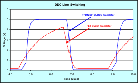
SCL_B or SDA_B Buffers of TPD12S015A Driving Long HDMI Cable (750-pF Load)

3 Description
The TPD12S015A device is an integrated HDMI companion chip solution. This device offers 8 low capacitance ESD clamps allowing HDMI 1.3/1.4 data rates. The 0.4-mm pitch DSBGA package pin mapping matches the HDMI Type D or Type C connectors. The integrated ESD clamps in monolithic silicon technology provide good matching between each differential signal pair. This provides an advantage over discrete ESD clamp solutions where variations between ESD clamps degrade the differential signal quality.
The TPD12S015A provides a regulated 5-V output (5VOUT) for sourcing the HDMI power line. The 5VOUT pin supplies minimum 55 mA to the HDMI receiver while meeting the HDMI 5VOUT specifications. The 5VOUT and the hot plug detect (HPD) circuitry are independent of the LS_OE control signal; they are controlled by the CT_CP_HPD pin. This independent control enables the detection scheme (5VOUT + HPD) to be active before enabling the HDMI link. The HPD_B port has a glitch filter to avoid false detection due to the bouncing while inserting the HDMI plug.
There are three noninverting bidirectional translation circuits for the SDA, SCL, and CEC lines; they are controlled by the LS_OE control signal. Each have a common power rail (VCCA) on the A side from 1.1 V to 3.6 V. On the B side, the SCL_B and SDA_B each have an internal 1.75-kΩ pullup connected to the regulated 5-V rail (5VOUT). The SCL and SDA pins meet the I2C specifications, and drive at least 750-pF loads which exceeds the HDMI cable specification. An LDO generates a 3.3-V internal rail for the CEC line operation when LS_OE = H & CT_CP_HPD = H. The CEC_B pin has a 26-kΩ pullup to this internal 3.3-V rail.
The TPD12S015A provides IEC61000-4-2 (Level 4) ESD protection. This device is offered in a space-saving 1.56-mm × 2.76-mm DSBGA package.
Device Information(1)
| PART NUMBER | PACKAGE | BODY SIZE (NOM) |
|---|---|---|
| TPD12S015A | DSBGA (28) | 1.56 mm × 2.76 mm |
- For all available packages, see the orderable addendum at the end of the data sheet.
4 Revision History
Changes from C Revision (March 2013) to D Revision
- Added ESD Ratings table, Thermal Information table, Feature Description section, Device Functional Modes, Application and Implementation section, Power Supply Recommendations section, Layout section, Device and Documentation Support section, and Mechanical, Packaging, and Orderable Information sectionGo
Changes from B Revision (April 2012) to C Revision