SLVS639F October 2007 – February 2016 TPD12S521
PRODUCTION DATA.
- 1 Features
- 2 Applications
- 3 Description
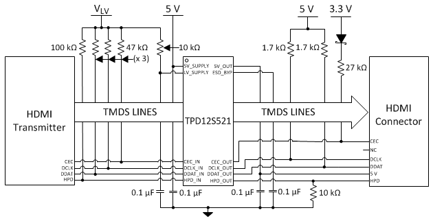
- 4 Circuit Protection Scheme
- 5 Revision History
- 6 Pin Configuration and Functions
- 7 Specifications
-
8 Detailed Description
- 8.1 Overview
- 8.2 Functional Block Diagram
- 8.3
Feature Description
- 8.3.1 Single-Chip ESD Solution for HDMI Driver
- 8.3.2 Supports All HDMI 1.3 and HDMI 1.4b Data Rates
- 8.3.3 Integrated Level Shifting for the Control Lines
- 8.3.4 ±8-kV Contact ESD Protection on External Lines
- 8.3.5 38-Pin TSSOP Provides Seamless Layout Option With HDMI Connector
- 8.3.6 Backdrive Protection
- 8.3.7 Lead-Free Package
- 8.3.8 On-Chip Current Regulator With 55-mA Current Output
- 8.4 Device Functional Modes
- 9 Application and Implementation
- 10Power Supply Recommendations
- 11Layout
- 12Device and Documentation Support
- 13Mechanical, Packaging, and Orderable Information
Package Options
Refer to the PDF data sheet for device specific package drawings
Mechanical Data (Package|Pins)
- DBT|38
Thermal pad, mechanical data (Package|Pins)
Orderable Information
1 Features
- IEC 61000-4-2 Level 4 ESD Protection
- Single-Chip ESD Solution for HDMI Driver
- On-Chip Current Regulator with 55-mA Current Output
- Supports All HDMI 1.3 and HDMI 1.4b Data Rates
(–3 dB Frequency > 3 GHz) - 0.8-pF Capacitance for the High Speed TMDS Lines
- 0.05-pF Matching Capacitance Between the Differential Signal Pair
- 38-Pin TSSOP Provides Seamless Layout Option with HDMI Connector
- Backdrive Protection
- TMDS_D[2:0]+/–
- TMDS_CK+/–
- CE_REMOTE_OUT
- DDC_DAT_OUT
- DDC_CLK_OUT
- HOTPLUG_DET_OUT
- Lead-Free Package
2 Applications
- PCs
- Consumer Electronics
- Set-Top Boxes
- DVD Players
3 Description
The TPD12S521 is a single-chip electro-static discharge (ESD) circuit protection device for the high-definition multimedia interface (HDMI) transmitter port. While providing ESD protection with transient voltage suppression (TVS) diodes, the TVS protection adds little or no additional glitch in the high-speed differential signals. The high-speed transition minimized differential signaling (TMDS) ESD protection lines add only 0.8-pF capacitance.
The low-speed control lines offer voltage-level shifting to eliminate the need for an external voltage level-shifter IC. The control line TVS diodes add 3.5-pF capacitance to the control lines. The 38-pin DBT package offers a seamless layout routing option to eliminate the routing glitch for the differential signal pairs. The DBT package pitch (0.5 mm) matches with the HDMI connector pitch. In addition, the pin mapping follows the same order as the HDMI connector pin mapping. The TPD12S521 provides an on-chip current limiting switch with output ratings of 55 mA at pin 38. This enables HDMI receiver detection even when the receiver device is powered off.
Device Information(1)
| PART NUMBER | PACKAGE | BODY SIZE (NOM) |
|---|---|---|
| TPD12S521 | TSSOP (38) | 6.40 mm × 9.70 mm |
- For all available packages, see the orderable addendum at the end of the datasheet.
4 Circuit Protection Scheme
