SLVSDL0A May 2016 – July 2016 TPD1E1B04
PRODUCTION DATA.
- 1 Features
- 2 Applications
- 3 Description
- 4 Revision History
- 5 Pin Configuration and Functions
- 6 Specifications
- 7 Detailed Description
- 8 Application and Implementation
- 9 Power Supply Recommendations
- 10Layout
- 11Device and Documentation Support
- 12Mechanical, Packaging, and Orderable Information
Package Options
Mechanical Data (Package|Pins)
- DPY|2
Thermal pad, mechanical data (Package|Pins)
- DPY|2
Orderable Information
1 Features
- IEC 61000-4-2 Level 4 ESD Protection
- ±30-kV Contact Discharge
- ±30-kV Air Gap Discharge
- IEC 61000-4-4 EFT Protection
- 80 A (5/50 ns)
- IEC 61000-4-5 Surge Protection
- 6.3 A (8/20 µs)
- IO Capacitance: 1 pF (Typical)
- DC Breakdown Voltage: 6.4 V (Typical)
- Low Leakage Current: 100 nA (Maximum)
- Extremely Low ESD Clamping Voltage
- 8.5 V at ±16-A TLP
- RDYN: 0.15 Ω
- Industrial Temperature Range: –40°C to +125°C
- Industry Standard 0402 Package
2 Applications
- End Equipment
- Wearables
- Laptops and Desktops
- Mobile and Tablets
- Set-Top Boxes
- DVR and NVR
- TV and Monitors
- EPOS (Electronic Point of Sale)
- Interfaces
- USB 2.0/1.1
- GPIO
- Pushbuttons
- Audio
3 Description
The TPD1E1B04 is a bidirectional TVS ESD protection diode featuring low RDYN and low clamping voltage. The TPD1E1B04 is rated to dissipate ESD strikes at the maximum level specified in the IEC 61000-4-2 international standard (Level 4).
The ultra-low dynamic resistance (0.15 Ω) and extremely low clamping voltage (8.5 V at 16-A TLP) ensure system level protection against transient events. This device features a 1-pF IO capacitance making it ideal for protecting interfaces such as USB 2.0.
The TPD1E1B04 is offered in the industry standard 0402 (DPY) package.
Device Information(1)
| PART NUMBER | PACKAGE | BODY SIZE (NOM) |
|---|---|---|
| TPD1E1B04 | X1SON (2) | 0.60 mm x 1.00 mm |
- For all available packages, see the orderable addendum at the end of the data sheet.
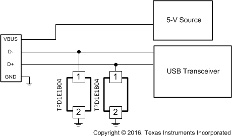
Typical USB 2.0 Application Schematic

4 Revision History
Changes from * Revision (May 2016) to A Revision
- Changed device status from Product Preview to Production DataGo