SLLSEH9B October 2013 – July 2016 TPD1S414
PRODUCTION DATA.
- 1 Features
- 2 Applications
- 3 Description
- 4 Revision History
- 5 Pin Configuration and Functions
-
6 Specifications
- 6.1 Absolute Maximum Ratings
- 6.2 ESD Ratings
- 6.3 Recommended Operating Conditions
- 6.4 Thermal Information
- 6.5 Electrical Characteristics (EN, ACK Pins)
- 6.6 Electrical Characteristics (OVP Circuit)
- 6.7 Timing Requirements
- 6.8 Switching Characteristics (nFET)
- 6.9 Supply Current Consumption
- 6.10 Thermal Shutdown Feature
- 6.11 Typical Characteristics
-
7 Detailed Description
- 7.1 Overview
- 7.2 Functional Block Diagram
- 7.3
Feature Description
- 7.3.1 Overvoltage Protection on VBUS_CON up to 30-V DC
- 7.3.2 Low RON nFET Switch Supports Host and Charging Mode
- 7.3.3 ±15-kV IEC 61000-4-2 Level 4 ESD Protection
- 7.3.4 100-V IEC 61000-4-5 µs Surge Protection
- 7.3.5 Start-Up and OVP Recovery Delay
- 7.3.6 Integrated Input Enable and Status Output Signal
- 7.3.7 Thermal Shutdown
- 7.4 Device Functional Modes
- 8 Application and Implementation
- 9 Power Supply Recommendations
- 10Layout
- 11Device and Documentation Support
- 12Mechanical, Packaging, and Orderable Information
Package Options
Refer to the PDF data sheet for device specific package drawings
Mechanical Data (Package|Pins)
- YZ|12
Thermal pad, mechanical data (Package|Pins)
Orderable Information
8 Application and Implementation
NOTE
Information in the following applications sections is not part of the TI component specification, and TI does not warrant its accuracy or completeness. TI’s customers are responsible for determining suitability of components for their purposes. Customers must validate and test their design implementation to confirm system functionality.
8.1 Application Information
The TPD1S414 device is added to a USB system to provide 30-V overvoltage protection, IEC 61000-4-2 ±15-kV contact/±15-kV air-gap protection, and IEC61000-4-5 100-V open-circuit surge protection. This protection is essential for USB systems as many USB charging PMICs cannot tolerate the high voltages that can occur in a USB system due to lightening surge, cable ringing, and ESD strikes. The following application example shows the typical system set-up used for TPD1S414.
8.2 Typical Application
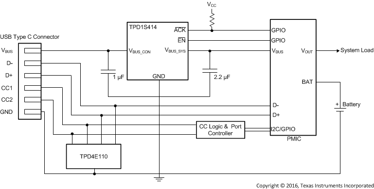
Figure 10 shows the typical system setup for TPD1S414, including external components required for proper functioning of the device.
 Figure 10. Typical Application Configuration for TPD1S414
8.2.1 Design Requirements
Table 3 lists the typical voltage values and external components used to operate the TPD1S414.
Table 3. Design Parameters
| DESIGN PARAMETERS | EXAMPLE VALUE |
|---|---|
| USB Signal range on VBUS_CON, VBUS_SYS | 4.4 V to 5.5 V |
| Operating current through VBUS | 3 A |
| Typical VBUS_CON Capacitance | 1 µF |
| Typical VBUS_SYS Capacitance | 2.2 µF |
| Drive EN low (enabled) | 0 V to 0.8 V |
| Drive EN high (disabled) | 1.2 V to 6 V |
8.2.2 Detailed Design Procedure
8.2.2.1 USB VBUS Voltage Range
The USB VBUS voltage range for a USB device operates between a minimum of 4.4 V and a maximum of 5.5 V (Legacy USB has a maximum of 5.25 V, but the new USB Type C standard raised the maximum to 5.5 V). The TPD1S414 is designed to operate with a VBUS_CON, VBUS_SYS voltage between 3.5 V and 5.9 V. This range exceeds the requirements for USB VBUS, allowing this device to be used in any USB system. Therefore, no special voltage precautions are necessary when adding TPD1S414 to a USB system.
8.2.2.2 USB VBUS Operating Current
In this application example, a VBUS current of 3 A is required. With the addition of the new USB Type C Standard, the VBUS operating current can vary anywhere from 0.5 A to 3 A, depending on the current capability advertised by the source on the CC pin. TPD1S414 is designed to operate up to a maximum of 3.5 A of current, allowing it to be used with the new USB Type C connector. TPD1S414 also has a low RON of 39 mΩ (typical), 50 mΩ (maximum), allowing for excellent thermal performance and low voltage drop across the switch at 3 A.
8.2.2.3 VBUS_CON and VBUS_SYS Capacitance
The USB standard requires a minimum capacitance of 1 µF on VBUS and allows for a maximum capacitance of 10 µF on a USB device. The minimum capacitance is to reduce inductive spiking on VBUS when disconnecting the charging cable, and the maximum capacitance is to put a limit on how much a device can drop the VBUS rail of its host when being hot-plugged into the system. This corresponds to having a typical capacitance of 1 µF on VBUS_CON for a USB system, but higher capacitance up to 10 µF can be used. No more than 10 µF must be put on VBUS_CON to ensure the USB specification is not violated. If more capacitance is required, place this on the VBUS_SYS pin. TPD1S414 turns on its nFET switch with a soft start to help pass USB in-rush compliance, so it is recommended to place bulk capacitance on the VBUS_SYS pin. External capacitors added to the VBUS_CON pin must be placed as close to the VBUS_CON pin as possible, and likewise external capacitors added to the VBUS_SYS pin must be placed as close to the VBUS_SYS pin as possible.
8.2.2.4 IEC 61000-4-5 100-V Open-Circuit Surge
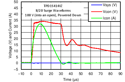
The IEC 61000-4-5 standard specifies the lightning and industrial surge model. Power lines like the VBUS line on the USB port are subject to switching and lightning transients. Power supply switching transients can enter the system due to capacitor bank switching on the rail, minor load switching on the system and various system faults like arcing to the grounding system of the installation. Direct lightning to the outer installations cause an overvoltage condition on the VBUS line. In the event of an overvoltage condition, the OVP block of the processor or the protection circuitry turns off isolating the system from these transients. Abruptly turning off the load, causes a further ripple due to the inductive nature of the charging cable. End systems require protection against these transients. These transients have greater energy than the ESD events. Systems cannot be protected from these transients using simple ESD diodes. The TPD1S414 has a precision trigger and precision clamping circuit that ensures a DC tolerance of 30 V while suppressing surge voltage up to 100 V under 35 V. Figure 11 shows the performance of TPD1S414 in the powered-down state under an 100-V surge pulse.
8.2.3 Application Curve
 Figure 11. TPD1S414 Response to an 100-V Surge