SLLSEH9B October 2013 – July 2016 TPD1S414
PRODUCTION DATA.
- 1 Features
- 2 Applications
- 3 Description
- 4 Revision History
- 5 Pin Configuration and Functions
-
6 Specifications
- 6.1 Absolute Maximum Ratings
- 6.2 ESD Ratings
- 6.3 Recommended Operating Conditions
- 6.4 Thermal Information
- 6.5 Electrical Characteristics (EN, ACK Pins)
- 6.6 Electrical Characteristics (OVP Circuit)
- 6.7 Timing Requirements
- 6.8 Switching Characteristics (nFET)
- 6.9 Supply Current Consumption
- 6.10 Thermal Shutdown Feature
- 6.11 Typical Characteristics
-
7 Detailed Description
- 7.1 Overview
- 7.2 Functional Block Diagram
- 7.3
Feature Description
- 7.3.1 Overvoltage Protection on VBUS_CON up to 30-V DC
- 7.3.2 Low RON nFET Switch Supports Host and Charging Mode
- 7.3.3 ±15-kV IEC 61000-4-2 Level 4 ESD Protection
- 7.3.4 100-V IEC 61000-4-5 µs Surge Protection
- 7.3.5 Start-Up and OVP Recovery Delay
- 7.3.6 Integrated Input Enable and Status Output Signal
- 7.3.7 Thermal Shutdown
- 7.4 Device Functional Modes
- 8 Application and Implementation
- 9 Power Supply Recommendations
- 10Layout
- 11Device and Documentation Support
- 12Mechanical, Packaging, and Orderable Information
Package Options
Refer to the PDF data sheet for device specific package drawings
Mechanical Data (Package|Pins)
- YZ|12
Thermal pad, mechanical data (Package|Pins)
Orderable Information
10 Layout
10.1 Layout Guidelines
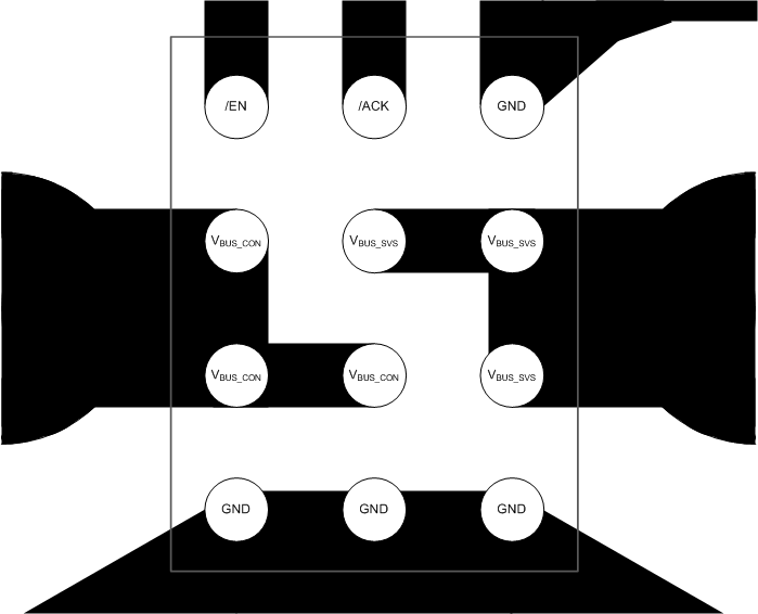
TPD1S414 can be routed in a single-layer PCB. PCB traces to VBUS_SYS, VBUS_CON, and GND can be routed in the fashion shown in Figure 12.
Shorting all of the VBUS_SYS pins together, all the VBUS_CON pins together, and all the GND pins together helps provide the lowest resistance between the USB connector and the PMIC. For this example, the trace widths to VBUS_SYS, VBUS_CON are 25 mils (0.635 mm) under TPD1S414. There are no VIAs required within the SMD pads in this design. Stitching VIAs for GND can be placed near the component instead.
The decoupling capacitors per the Recommended Operating Conditions must be placed as close as possible to the TPD1S414. There must be a short path from the device ground pins to the system ground plane. This ensures best protection under ESD and surge transients.
10.2 Layout Example
 Figure 12. TPD1S414 Layout Example