SLLSEH9B October 2013 – July 2016 TPD1S414
PRODUCTION DATA.
- 1 Features
- 2 Applications
- 3 Description
- 4 Revision History
- 5 Pin Configuration and Functions
-
6 Specifications
- 6.1 Absolute Maximum Ratings
- 6.2 ESD Ratings
- 6.3 Recommended Operating Conditions
- 6.4 Thermal Information
- 6.5 Electrical Characteristics (EN, ACK Pins)
- 6.6 Electrical Characteristics (OVP Circuit)
- 6.7 Timing Requirements
- 6.8 Switching Characteristics (nFET)
- 6.9 Supply Current Consumption
- 6.10 Thermal Shutdown Feature
- 6.11 Typical Characteristics
-
7 Detailed Description
- 7.1 Overview
- 7.2 Functional Block Diagram
- 7.3
Feature Description
- 7.3.1 Overvoltage Protection on VBUS_CON up to 30-V DC
- 7.3.2 Low RON nFET Switch Supports Host and Charging Mode
- 7.3.3 ±15-kV IEC 61000-4-2 Level 4 ESD Protection
- 7.3.4 100-V IEC 61000-4-5 µs Surge Protection
- 7.3.5 Start-Up and OVP Recovery Delay
- 7.3.6 Integrated Input Enable and Status Output Signal
- 7.3.7 Thermal Shutdown
- 7.4 Device Functional Modes
- 8 Application and Implementation
- 9 Power Supply Recommendations
- 10Layout
- 11Device and Documentation Support
- 12Mechanical, Packaging, and Orderable Information
Package Options
Refer to the PDF data sheet for device specific package drawings
Mechanical Data (Package|Pins)
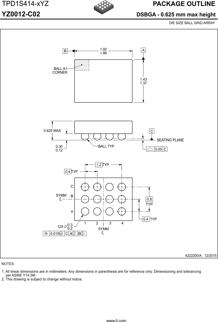
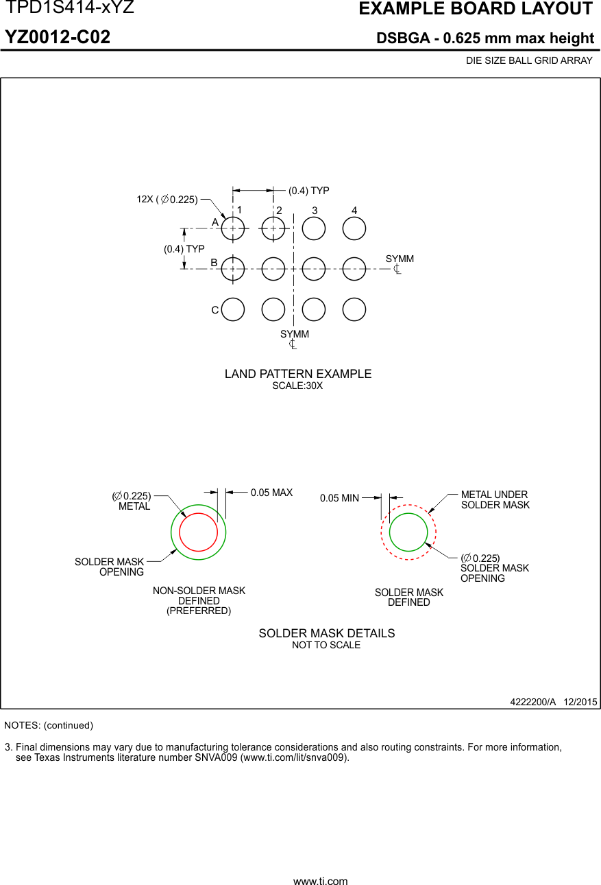
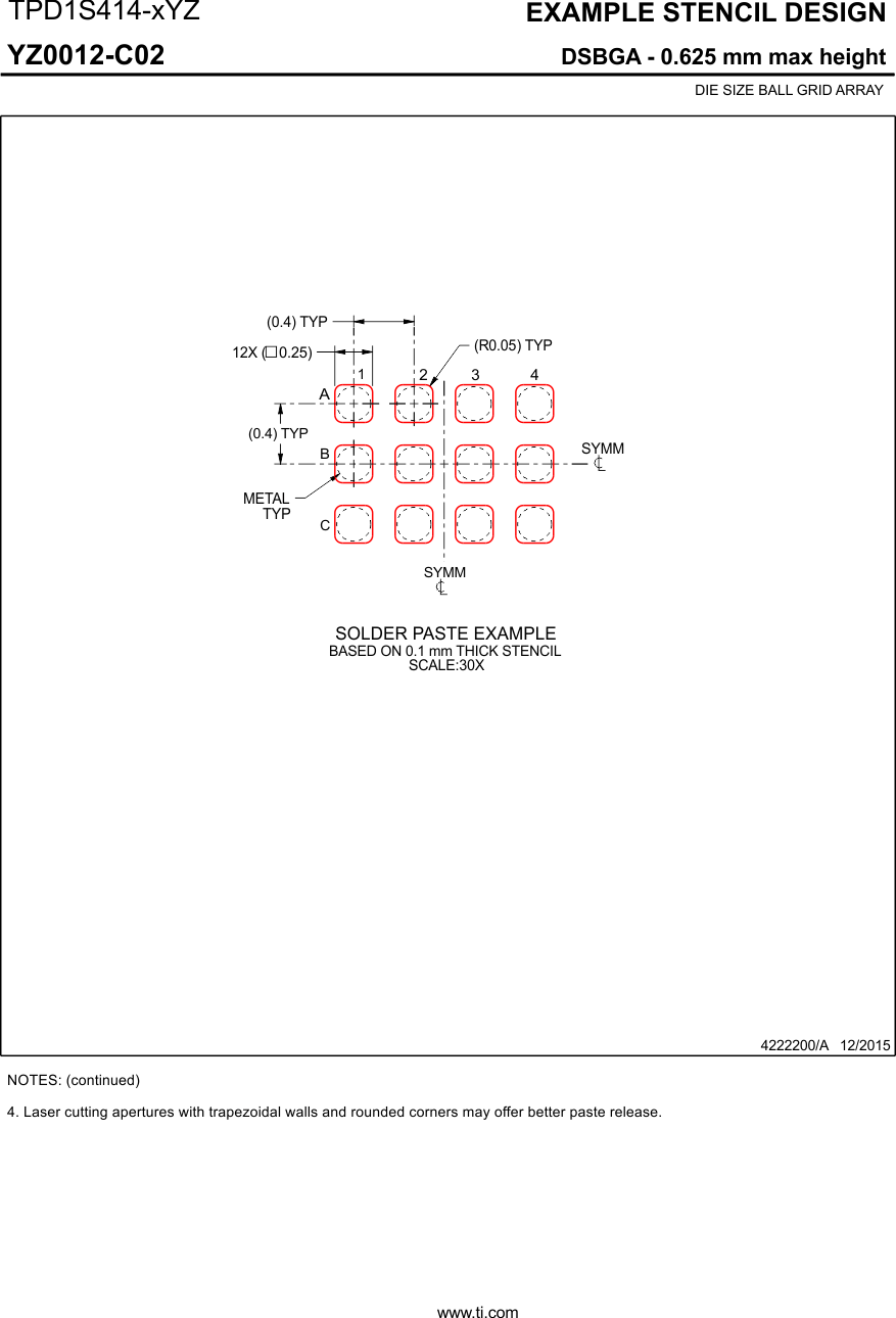
- YZ|12
Thermal pad, mechanical data (Package|Pins)
Orderable Information
12 Mechanical, Packaging, and Orderable Information
The following pages include mechanical, packaging, and orderable information. This information is the most current data available for the designated devices. This data is subject to change without notice and revision of this document. For browser-based versions of this data sheet, refer to the left-hand navigation.


