SLLSEH9B October 2013 – July 2016 TPD1S414
PRODUCTION DATA.
- 1 Features
- 2 Applications
- 3 Description
- 4 Revision History
- 5 Pin Configuration and Functions
-
6 Specifications
- 6.1 Absolute Maximum Ratings
- 6.2 ESD Ratings
- 6.3 Recommended Operating Conditions
- 6.4 Thermal Information
- 6.5 Electrical Characteristics (EN, ACK Pins)
- 6.6 Electrical Characteristics (OVP Circuit)
- 6.7 Timing Requirements
- 6.8 Switching Characteristics (nFET)
- 6.9 Supply Current Consumption
- 6.10 Thermal Shutdown Feature
- 6.11 Typical Characteristics
-
7 Detailed Description
- 7.1 Overview
- 7.2 Functional Block Diagram
- 7.3
Feature Description
- 7.3.1 Overvoltage Protection on VBUS_CON up to 30-V DC
- 7.3.2 Low RON nFET Switch Supports Host and Charging Mode
- 7.3.3 ±15-kV IEC 61000-4-2 Level 4 ESD Protection
- 7.3.4 100-V IEC 61000-4-5 µs Surge Protection
- 7.3.5 Start-Up and OVP Recovery Delay
- 7.3.6 Integrated Input Enable and Status Output Signal
- 7.3.7 Thermal Shutdown
- 7.4 Device Functional Modes
- 8 Application and Implementation
- 9 Power Supply Recommendations
- 10Layout
- 11Device and Documentation Support
- 12Mechanical, Packaging, and Orderable Information
Package Options
Refer to the PDF data sheet for device specific package drawings
Mechanical Data (Package|Pins)
- YZ|12
Thermal pad, mechanical data (Package|Pins)
Orderable Information
6 Specifications
6.1 Absolute Maximum Ratings
over operating free-air temperature range (unless otherwise noted)(1)(2)(1) Stresses beyond those listed under Absolute Maximum Ratings may cause permanent damage to the device. These are stress ratings only, which do not imply functional operation of the device at these or any other conditions beyond those indicated under Recommended Operating Conditions. Exposure to absolute-maximum-rated conditions for extended periods may affect device reliability.
(2) The algebraic convention, whereby the most negative value is a minimum and the most positive value is a maximum.
6.2 ESD Ratings
| VALUE | UNIT | ||||
|---|---|---|---|---|---|
| V(ESD) | Electrostatic discharge | Human-body model (HBM), per ANSI/ESDA/JEDEC JS-001(1) | ±2000 | V | |
| Charged-device model (CDM), per JEDEC specification JESD22-C101(2) | ±1000 | ||||
| IEC 61000-4-2 contact discharge | ±15000 | V | |||
| IEC 61000-4-2 air-gap discharge | ±15000 | V | |||
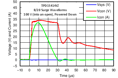
| IEC 61000-4-5 Peak Pulse Current (tp = 8/20 µs) | VBUS_CON pin | 21 | A | ||
| IEC 61000-4-5 Peak Pulse Power (tp = 8/20 µs) | VBUS_CON pin | 700 | W | ||
| IEC 61000-4-5 Open circuit voltage (tp = 1.2/50 µs) | VBUS_CON pin | 100 | V | ||
(1) JEDEC document JEP155 states that 500-V HBM allows safe manufacturing with a standard ESD control process. Pins listed as
±2000 V may actually have higher performance.
±2000 V may actually have higher performance.
(2) JEDEC document JEP157 states that 250-V CDM allows safe manufacturing with a standard ESD control process. Pins listed as
±1000 V may actually have higher performance.
±1000 V may actually have higher performance.
6.3 Recommended Operating Conditions
over operating free-air temperature range (unless otherwise noted)| PARAMETER | MIN | NOM | MAX | UNIT | ||
|---|---|---|---|---|---|---|
| VBUS_CON | Supply voltage from USB connector | 5.9 | V | |||
| VBUS_SYS | Internal supply DC voltage rail on the PCB | 5.9 | V | |||
| CLOAD | Output load capacitance | VBUS_SYS pin | 2.2 | µF | ||
| CIN | Input capacitance | VBUS_CON pin | 1 | µF | ||
| RPULLUP | Pullup resistor | ACK pin | 4.3 | 100 | kΩ | |
| IVBUS | Continuous current on VBUS_CON and VBUS_SYS pins | VBUS_CON
VBUS_SYS |
3.5 | A | ||
| IDIODE | Continuous current through the FET body diode | 1 | A | |||
6.4 Thermal Information
| THERMAL METRIC(1) | TPD1S414 | UNIT | |
|---|---|---|---|
| YZ (DSBGA) | |||
| 12 PINS | |||
| RθJA | Junction-to-ambient thermal resistance | 89 | °C/W |
| RθJC(top) | Junction-to-case(top) thermal resistance | 0.6 | °C/W |
| RθJB | Junction-to-board thermal resistance | 16.3 | °C/W |
| ψJT | Junction-to-top characterization parameter | 2.7 | °C/W |
| ψJB | Junction-to-board characterization parameter | 16.2 | °C/W |
| RθJC(bot) | Junction-to-case(bottom) thermal resistance | n/A | °C/W |
(1) For more information about traditional and new thermal metrics, see the Semiconductor and IC Package Thermal Metrics application report.
6.5 Electrical Characteristics (EN, ACK Pins)
over operating free-air temperature range (unless otherwise noted)| PARAMETER | TEST CONDITIONS | MIN | TYP | MAX | UNIT | |
|---|---|---|---|---|---|---|
| VIH | High-level input voltage, EN | 1.2 | 6 | V | ||
| VIL | Low-level input voltage, EN | 0.8 | V | |||
| IIL | Input leakage current EN | VI = 3.3 V | 1 | µA | ||
| VOL | Low-level output voltage, ACK | IOL = 3 mA | 0.4 | V | ||
6.6 Electrical Characteristics (OVP Circuit)
over operating free-air temperature range (unless otherwise noted)| PARAMETER | TEST CONDITIONS | MIN | TYP | MAX | UNIT | |
|---|---|---|---|---|---|---|
| VOVP_RISING | Input overvoltage protection threshold, VBUS_CON | VBUS_CON increasing from 5 V | 6 | 6.2 | 6.4 | V |
| VHYS_OVP | Hysteresis on OVP, VBUS_CON | VBUS_CON decreasing from 7 V to 5 V | 50 | mV | ||
| VOVP_FALLING | Input overvoltage protection threshold, VBUS_CON | VBUS_CON decreasing from 7 V to 5 V | 5.93 | 6.37 | V | |
| VUVLO | Input undervoltage lockout, VBUS_CON | VBUS_CON voltage rising from 0 V to 5 V | 3.1 | 3.3 | 3.5 | V |
| VHYS_UVLO | Hysteresis on UVLO, VBUS_CON | Difference between rising and falling UVLO thresholds | 100 | mV | ||
| VUVLO_FALLING | Input undervoltage lockout, VBUS_CON | VBUS_CON voltage rising from 5 V to 0 V | 3 | 3.2 | 3.4 | V |
| VUVLO_SYS | VBUS_SYS undervoltage lockout, VBUS_SYS | VBUS_SYS voltage rising from 0 V to 5 V | 3.1 | 3.6 | 4.3 | V |
| VHYS_UVLO_SYS | VBUS_SYS UVLO Hysteresis, VBUS_SYS | Difference between rising and falling UVLO thresholds on VBUS_SYS | 480 | mV | ||
| VUVLO_SYS_FALL | VBUS_SYS undervoltage lockout, VBUS_SYS | VBUS_SYS voltage falling from 7 V to 5 V | 3 | 3.2 | 3.4 | V |
6.7 Timing Requirements
over operating free-air temperature range (unless otherwise noted)| MIN | NOM | MAX | UNIT | |||
|---|---|---|---|---|---|---|
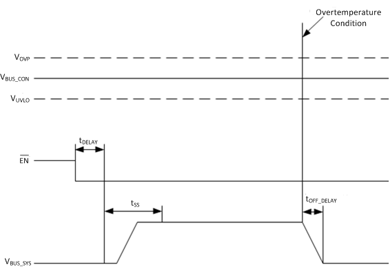
| tDELAY | USB charging turnon delay | Measured from EN asserted LOW to nFET beginning to Turn ON(1) excluding soft-start time | 20 | ms | ||
| tSS | USB charging rise time (soft-start delay) | Measure from VBUS_SYS rises above 25% (with 1-MΩ load/ NO CLOAD) until ACK goes Low (10%) | 25 | ms | ||
| tOFF_DELAY | USB charging turnoff time | Measured from EN asserted High to VBUS_SYS falling to 10% with RLOAD = 10 Ω and No CLOAD on VBUS_SYS | 4 | µs | ||
| OVERVOLTAGE PROTECTION | ||||||
| tOVP_response | OVP response time | Measured from OVP Condition to FET Turn OFF(2). VBUS_CON rises at 1V / 100 ns | 100 | ns | ||
| tOVP_Recov | Recovery time | Measured from OVP Clear to FET Turn ON(3) | 20 | ms | ||
(1) Shown in Figure 1.
(2) Parameters provided for reference only, and do not constitute part of TI's published device specifications for purposes of TI's product warranty.
(3) Excludes soft-start time
6.8 Switching Characteristics (nFET)
over operating free-air temperature range (unless otherwise noted)| PARAMETER | TEST CONDITIONS | MIN | TYP | MAX | UNIT | |
|---|---|---|---|---|---|---|
| RDS(on) | Switch ON-resistance | VBUS_CON = 5 V, IOUT = 1 A, TA = 25˚C |
39 | 50 | mΩ | |
6.9 Supply Current Consumption
over operating free-air temperature range (unless otherwise noted)6.10 Thermal Shutdown Feature
over operating free-air temperature range (unless otherwise noted)| PARAMETER | TEST CONDITIONS | MIN | TYP | MAX | UNIT | |
|---|---|---|---|---|---|---|
| TSHDN | Thermal shutdown | Junction temperature | 145 | °C | ||
| Thermal-shutdown hysteresis | Junction temperature | 35 | °C | |||
6.11 Typical Characteristics
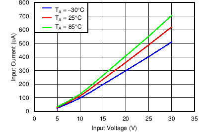 Figure 2. Input Supply Current vs Supply Voltage
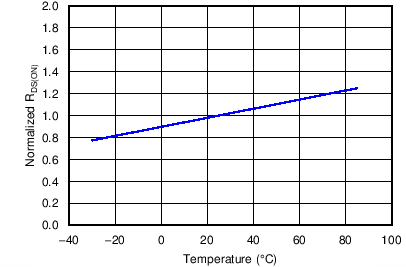
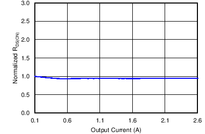 Figure 4. Normalized RDS(ON) vs Output Current
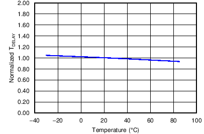 Figure 6. Normalized TDELAY
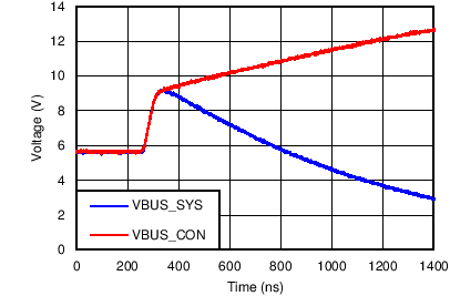
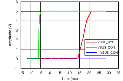 Figure 8. Power Up With 2.2 µF on VBUS_SYS
