SLVS953B June 2009 – August 2015 TPD2E009
PRODUCTION DATA.
- 1 Features
- 2 Applications
- 3 Description
- 4 Revision History
- 5 Pin Configuration and Functions
- 6 Specifications
- 7 Detailed Description
- 8 Application and Implementation
- 9 Power Supply Recommendations
- 10Layout
- 11Device and Documentation Support
- 12Mechanical, Packaging, and Orderable Information
Package Options
Mechanical Data (Package|Pins)
Thermal pad, mechanical data (Package|Pins)
- DRT|3
Orderable Information
10 Layout
10.1 Layout Guidelines
Layout considerations such as package selection, trace routing, and so forth, must be accounted for while designing the ESD clamp circuit for a high-speed interface. Difficult routing can lead the designer to use vias or stubs in the board traces, which creates significant disruption in the line impedance in the high-speed signal path. Poor package choice can force the designer to route differential traces with unequal lengths and add the skew in the signals. TI recommends coupling the differential traces closely to reduce the EMI interference.
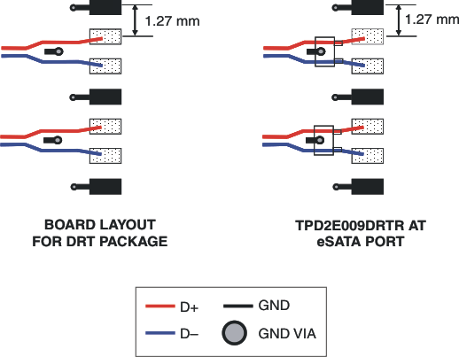
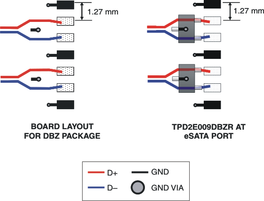
The TPD2E009 can provide system-level ESD protection to the high-speed differential ports (up to 6-Gbps data rate). The flow-through package offers flexibility for board routing with traces up to 15 mils (0.38 mm) wide. Figure 14 and Figure 15 show the board layout scheme for the D+ and D– lines of a single differential pair, which allows the differential signal pairs to couple together right after they touch the ESD ports (pin 1 and pin 2) of the TPD2E009.
10.2 Layout Examples
 Figure 14. TPD2E009DRTR at eSATA Connector Interface
 Figure 15. TPD2E009DBZR at eSATA Connector Interface