SLVS817G May 2008 – June 2015 TPD4S009 , TPD4S010
PRODUCTION DATA.
- 1 Features
- 2 Applications
- 3 Description
- 4 Revision History
- 5 Pin Configuration and Functions
- 6 Specifications
-
7 Detailed Description
- 7.1 Overview
- 7.2 Functional Block Diagram
- 7.3
Feature Description
- 7.3.1 ±8-kV IEC61000-4-2 Level 4 Contact ESD Protection
- 7.3.2 IEC61000-4-5 Surge Protection
- 7.3.3 I/O Capacitance
- 7.3.4 Low Leakage Current
- 7.3.5 Supports High-Speed Differential Data Rates
- 7.3.6 Ultra-low Matching Capacitance Between Differential Signal Pairs
- 7.3.7 Ioff Feature for the TPD4S009
- 7.3.8 Industrial Temperature Range
- 7.3.9 Easy Flow-Through Routing
- 7.4 Device Functional Modes
- 8 Application and Implementation
- 9 Power Supply Recommendations
- 10Layout
- 11Device and Documentation Support
- 12Mechanical, Packaging, and Orderable Information
Package Options
Mechanical Data (Package|Pins)
Thermal pad, mechanical data (Package|Pins)
Orderable Information
7 Detailed Description
7.1 Overview
The TPD4S009 and TPD4S010 are four-channel TVS diode arrays for electrostatic discharge (ESD) protection. TPD4S009 and TPD4S010 are rated to dissipate contact ESD strikes at the maximum level specified in the IEC 61000-4-2 international standard (Level 4), with ±8-kV contact discharge ESD protection. The low 0.8 pF capacitance of these devices, coupled with the excellent matching between differential signal pairs (0.05-pF line-line capacitance for the TPD4S009DRY) enables this device to operate at high-speed differential data rates (3-dB bandwidth > 4 GHz).
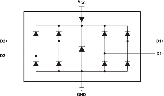
The TPD4S009 offers an optional VCC supply pin which can be connected to system supply plane. There is a blocking diode at the VCC pin to enable the Ioff feature for the TPD4S009. The TPD4S009 can handle live signal at the D+, D- pins when the VCC pin is connected to zero volt. The VCC pin allows all the internal circuit nodes of the TPD4S009 to be at known potential during start up time. However, connecting the optional VCC pin to board supply plane doesn't affect the system level ESD performance of the TPD4S009. The TPD4S010 does not offer the VCC pin.
7.2 Functional Block Diagram
 Figure 6. TPD4S009
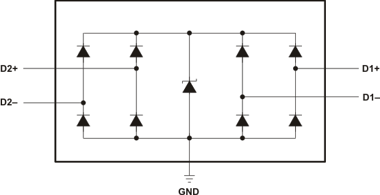
 Figure 7. TPD4S010
7.3 Feature Description
7.3.1 ±8-kV IEC61000-4-2 Level 4 Contact ESD Protection
The I/O pins can withstand ESD events up to ±8-kV contact and ±9-kV air. An ESD/surge clamp diverts the current to ground.
7.3.2 IEC61000-4-5 Surge Protection
The I/O pins can withstand surge events up to 2.5 A and 25 W (8/20 µs waveform). An ESD/surge clamp diverts this current to ground.
7.3.3 I/O Capacitance
The capacitance between each I/O pin to ground is 0.8 pF (typical) for both TPD4S009 and TPD4S010. These devices support data rates up to 3.4 Gbps.
7.3.4 Low Leakage Current
The I/O pins feature a low leakage current of 10 nA (typical) with an IO bias of 3.3 V and VCC bias of 5V.
7.3.5 Supports High-Speed Differential Data Rates
The I/O pins low capacitance of 0.8 pF (typical) gives them a typical –3 dB bandwidth > 4GHz. This allows TPD4S009 and TPD4S010 to protect interfaces with high speed signals like HDMI 1.4.
7.3.6 Ultra-low Matching Capacitance Between Differential Signal Pairs
The monolithic silicon technology allows matching between the differential signal pairs. The excellent matching between the differential pair signal lines (0.05-pF line-line capacitance for the TPD4S009DRY) enables this device to operate at high-speed differential data rates (3-dB bandwidth > 4 GHz). Excellent matching capacitance between differential signal pairs is also crucial to minimize the inter-pair and intra-pair skew between differential signals, which is crucial for many high-speed signal interfaces like HDMI 1.4.
7.3.7 Ioff Feature for the TPD4S009
The TPD4S009 offers an optional VCC supply pin which can be connected to system supply plane. There is a blocking diode at the VCC pin which makes it so the TPD4S009 can handle live signal at the D+, D- pins when the VCC pin is connected to zero volt. This is the Ioff feature, which is crucial for HDMI, as a live signal can be put on the IO pins when the system is powered off. The TPD4S010 does not offer the VCC pin.
7.3.8 Industrial Temperature Range
This device features an industrial operating range of –40°C to 85°C.
7.3.9 Easy Flow-Through Routing
The layout of this device makes it simple and easy to add protection to an existing layout. The packages offers flow-through routing, requiring minimal modification to an existing layout. Flow-through routing also allows the PCB designer to optimize the signal integrity of any high-speed signals being protected.
7.4 Device Functional Modes
TPD4S009 and TPD4S010 are passive integrated circuits that trigger when voltages are above VBR or below the lower diodes Vf (–0.6 V). During ESD events, voltages as high as ±8 kV (contact) can be directed to ground via the internal diode network. Once the voltages on the protected line fall below the trigger levels of TPD4S009 or TPD4S010 (usually within 10’s of nano-seconds) the device reverts back to its high-impedance state.