SLVS928B March 2009 – August 2014 TPD4S012
UNLESS OTHERWISE NOTED, this document contains PRODUCTION DATA.
- 1 Features
- 2 Applications
- 3 Description
- 4 Revision History
- 5 Pin Configurations and Functions
- 6 Specifications
- 7 Detailed Description
- 8 Applications and Implementation
- 9 Power Supply Recommendations
- 10Layout
- 11Device and Documentation Support
- 12Mechanical, Packaging, and Orderable Information
Package Options
Mechanical Data (Package|Pins)
- DRY|6
Thermal pad, mechanical data (Package|Pins)
- DRY|6
Orderable Information
8 Applications and Implementation
8.1 Application Information
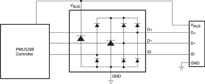
The TPD4S012 is a four-channel Transient Voltage Suppressor (TVS) based Electrostatic Discharge (ESD) protection diode array for USB chargers and USB On-The-Go (OTG) interfaces.
The TPD4S012 provides IEC 61000-4-2 system level ESD Protection featuring 15 V tolerance on the VBUS line. The device is ideal for providing circuit protection for USB charger and OTG applications due to its high-voltage tolerance at the VBUS line and small flow-through package.
8.2 Typical Application
8.2.1 Design Requirements
For this design example, a single TPD4S012 is used to protect all pins of a micro/mini USB connector.
Given the USB application, the following parameters are known.
| DESIGN PARAMETER | VALUE |
|---|---|
| Signal range on D+, D–, and ID | 0 V to 5 V |
| Signal range on VBUS | 0 V to 5 V |
| Operating Frequency | 240 MHz |
8.2.2 Detailed Design Procedure
To begin the design process, some parameters must be decided upon; the designer needs to know the following:
- Signal range on all the protected lines
- Operating frequency
8.2.2.1 Signal Range on D+, D-, ID and VBUS pins
The TPD4S012 has 3 pins which support 0 to 5.5 V signals, these are suited for the D+, D–, and ID pins. The VBUS pin is suitable for the VBUS line, and has the benefit of being tolerant of voltages up to 16 V
8.2.2.2 Operating Frequency
The 0.8 pF (Typ) of the TPD4S012 support data rates in excess of 480 Mbps.
8.2.3 Application Curve
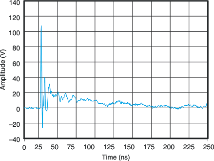 Figure 12. IEC Clamping Waveform, 8 kV Contact, D+, 25 ns/div
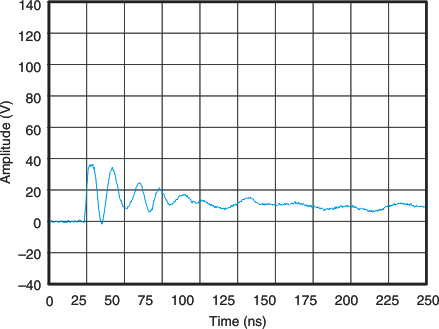 Figure 14. VBUS IEC Clamping Waveform, 8 kV Contact, 25 ns/div
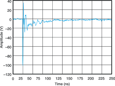 Figure 13. IEC Clamping Waveform, –8 kV Contact, D+, 25 ns/div
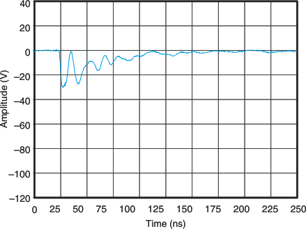 Figure 15. VBUS IEC Clamping Waveform, –8 kV Contact, 25 ns/div